
User guide
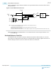
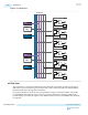

The receiver input pin drives the reference clock network, which can then feed any number of transmitter
PLLs on the same side of the device. When a receiver input pin is used as an input reference clock source,
the clock data recovery (CDR) block of that channel is not available. As indicated in Figure 3-5, only one
RX differential pin pair per three channels can be used as an input reference clock source at any given
time.
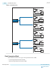
PLL Cascading as an Input Reference Clock Source
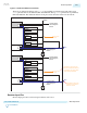
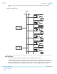
In PLL cascading, PLL outputs are connected to the feedback and cascading clock network. The input
reference clock to the first PLL can be sourced from the same network. In this mode, the output of one
PLL drives the reference clock input of another PLL. PLL cascading can generate frequency outputs not
normally possible with a single PLL solution. The transceivers in Arria 10 devices support fPLL to fPLL or
fPLL to ATX PLL cascading.
Note:
Due to pending silicon characterization, Altera does not recommend using PLL cascading in ACDS
14.0 Arria 10 edition, 14.1, and 15.0 Arria 10 versions of the Quartus
®
II software.
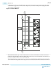
Reference Clock Network
The reference clock network distributes a reference clock source to either the entire left or right side of the
FPGA where the transceivers reside. This allows any reference clock pin to drive any transmitter PLL on
the same side of the device. Designs using multiple transmitter PLLs which require the same reference
clock frequency and are located along the same side of the device, can share the same dedicated reference
clock (refclk) pin.
Global Clock or Core Clock as an Input Reference Clock
The global clock or the core clock can be used as an input reference clock for any PLL type.
The global or core clock network routes the clock directly to the PLL. In this case the PLL reference clock
network is not used. For best performance, use the dedicated reference clock pins or the reference clock
network.
Transmitter Clock Network
The transmitter clock network routes the clock from the transmitter PLL to the transmitter channel. It
provides two types of clocks to the transmitter channel:
• High Speed Serial clock – high speed clock for the serializer.
• Low Speed Parallel clock – low speed clock for the serializer and the PCS.
In a bonded channel configuration, both the serial clock and the parallel clock are routed from the
transmitter PLL to the transmitter channel. In a non-bonded channel configuration, only the serial clock
is routed to the transmitter channel, and the parallel clock is generated locally within the channel. To
support various bonded and non-bonded clocking configurations, four types of transmitter clock network
lines are available:
• x1 clock lines
• x6 clock lines
• xN clock lines
• GT clock lines
3-30
PLL Cascading as an Input Reference Clock Source
UG-01143
2015.05.11
Altera Corporation
PLLs and Clock Networks
Send Feedback