
User guide
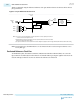
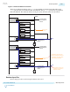
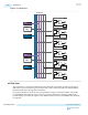
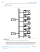
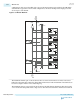
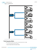

Figure 3-6: Dedicated Reference Clock Pins
There are two dedicated reference clock (refclk) pins available in each transceiver bank. The bottom
refclk pin feeds the bottom ATX PLL, fPLL and CMU PLL. The top refclk pin feeds the top ATX PLL,
fPLL and CMU PLL. The dedicated reference clock pins can also drive the reference clock network.
Refclk
CH5
CMU PLL
CH4
CDR PLL
CH3
fPLL1
ATX PLL1
CDR PLL
From PLL Feedback
and Cascading Clock
Network
From PLL Feedback
and Cascading Clock
Network
Refclk
CH2
CMU PLL
CH1
CDR PLL
CH0
fPLL0
ATX PLL0
CDR PLL
Reference Clock
Network
Reference Clock
Network
Reference Clock
Network
Input Reference Clock to the PLLs
Can Come from Either the Reference
Clock Network or the PLL Feedback
and Cascading Clock Network
ATX and fPLL Can Receive the
Input Reference Clock from a
Dedicated refclk Pin
From PLL Feedback
and Cascading Clock
Network
From PLL Feedback
and Cascading Clock
Network
Receiver Input Pins
Receiver input pins can be used as an input reference clock source.
UG-01143
2015.05.11
Receiver Input Pins
3-29
PLLs and Clock Networks
Altera Corporation
Send Feedback