
User guide

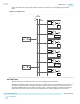


Altera recommends using the dedicated reference clock pins and the reference clock network for the best
jitter performance.
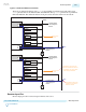
Figure 3-5: Input Reference Clock Sources
Dedicated
refclk
pin
RX pin 2
RX pin 1
Note : (1) You can choose only one of the three RX pins to be used as an input reference clock source. Any RX pin on the same side
of the device can be used as an input reference clock.
RX pin 0
Reference Clock
Network
Serial Clock
Fractional
PLL
ATX PLL,
Channel PLL
(CMU PLL/CDR),
or fPLL
Input
Reference
Clock
(2)
(3)
(2) Dedicated refclk pin can be used as an input reference clock source only for ATX or fPLL or to the reference clock network.
Reference clock network can then drive the CMU PLL.
(3) The output of another PLL can be used as an input reference clock source during PLL cascading. Arria 10 transceivers support fPLL to fPLL, fPLL to ATX PLL, and fPLL to CMU cascading.
(1)
(fPLL)
Global or
Core Clock
Note: In Arria 10 devices, the FPGA fabric core clock network can be used as an input reference source
for any PLL type.
Dedicated Reference Clock Pins
To minimize the jitter, the advanced transmit (ATX) PLL and the fractional PLL (fPLL) can source the
input reference clock directly from the reference clock buffer without passing through the reference clock
network. The input reference clock is also fed into the reference clock network.
3-28
Dedicated Reference Clock Pins
UG-01143
2015.05.11
Altera Corporation
PLLs and Clock Networks
Send Feedback