
User guide

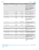
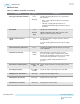
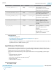

Port Range Clock Domain Description
reconfig_address0[9:0] input reconfig_clk0 10-bit address bus used to
specify address to be accessed for
both read and write operations.
reconfig_writedata0[31:0] input reconfig_clk0 32-bit data bus. Carries the write
data to the specified address.
reconfig_readdata0[31:0] output reconfig_clk0 32-bit data bus. Carries the read
data from the specified address.
reconfig_waitrequest0 output reconfig_clk0 Indicates when the Avalon
interface signal is busy. When
asserted, all inputs must be held
constant.
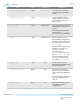
pll_cal_busy output Asynchronous Status signal that is asserted high
when PLL calibration is in
progress.
Perform logical OR with this
signal and the tx_cal_busy port
on the reset controller IP.
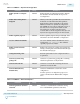
Related Information
• Calibration on page 1-24
• Reconfiguration Interface and Dynamic Reconfiguration on page 6-1
• Avalon Interface Specifications
The ports related to reconfiguration are compliant with the Avalon Specification. Refer to the Avalon
Specification for more details about these ports.
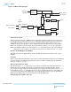
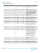
Input Reference Clock Sources
The transmitter PLL and the clock data recovery (CDR) block need an input reference clock source to
generate the clocks required for transceiver operation. The input reference clock must be stable and free-
running at device power-up for proper PLL calibrations.
Arria 10 transceiver PLLs have five possible input reference clock sources, depending on jitter require‐
ments:
• Dedicated reference clock pins
• Reference clock network
• The output of another fPLL with PLL cascading
(50)
• Receiver input pins
• Global clock or core clock
(50)
(50)
Not available for CMU
UG-01143
2015.05.11
Input Reference Clock Sources
3-27
PLLs and Clock Networks
Altera Corporation
Send Feedback