
User guide

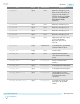
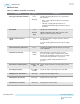
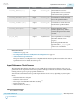

Port Range Clock Domain Description
pcie_sw[1:0] input Asynchronous 2-bit rate switch control input
used for PCIe protocol
implementation.
pcie_sw_done[1:0] output Asynchronous 2-bit rate switch status output
used for PCIe protocol
implementation.
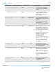
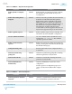
atx_to_fpll_cascade_clk
input N/A
Enables fPLL to ATX PLL
cascading clock output port.
fpll_to_fpll_cascade_clk
output N/A
fPLL to fPLL cascade output
port (only in Core mode)
active_clk
output N/A Creates an output signal that
indicates the input clock being
used by the PLL. A logic Low
on this signal indicates
refclk0 is being used and a
logic High indicates refclk1 is
being used (only in Core mode
with Clock Switchover
enabled)
Related Information
• Calibration on page 1-24
• Reconfiguration Interface and Dynamic Reconfiguration on page 6-1
• Avalon Interface Specifications
The ports related to reconfiguration are compliant with the Avalon Specification. Refer to the Avalon
Specification for more details about these ports.
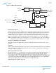
CMU PLL
The clock multiplier unit (CMU) PLL resides locally within each transceiver channel. The channel PLL's
primary function is to recover the receiver clock and data in the transceiver channel. In this case the PLL
is used in clock and data recovery (CDR) mode.
When the channel PLL of channels 1 and 4 is configured in the CMU mode, the channel PLL can drive
the local clock generation block (CGB) of its own channel. However, when the channel PLL is used as a
CMU PLL, the channel can only be used because a transmitter channel as the CDR block is not available
to recover the received clock and data.
The CMU PLL from transceiver channel 1 and channel 4 can also be used to drive other transceiver
channels within the same transceiver bank. The CDR of channels 0, 2, 3, and 5 cannot be configured as a
CMU PLL.
UG-01143
2015.05.11
CMU PLL
3-21
PLLs and Clock Networks
Altera Corporation
Send Feedback