
User guide
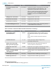
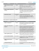
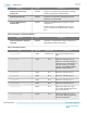
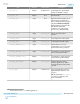
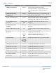
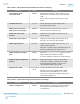

Table 3-8: fPLL—Master Clock Generation Block Parameters and Settings
Parameters Range Description
Include Master Clock
Generation Block
On/Off When enabled, includes a master CGB as a part of
the fPLL IP core. The PLL output drives the master
CGB.
This is used for x6/xN bonded and non-bonded
modes.
Clock division factor 1, 2, 4, 8 Divides the master CGB clock input before
generating bonding clocks.
Enable x6/xN non-bonded
high-speed clock output port
On/Off Enables the master CGB serial clock output port
used for x6/xN non-bonded modes.
Enable PCIe clock switch
interface
On/Off Enables the control signals used for PCIe clock
switch circuitry.
MCGB input clock frequency Read only Displays the master CGB’s required input clock
frequency. You cannot set this parameter.
MCGB output data rate Read only Displays the master CGB’s output data rate. You
cannot set this parameter.
This value is calculated based on MCGB input clock
frequency and MCGB clock division factor.
Enable bonding clock output
ports
On/Off Enables the tx_bonding_clocks output ports of the
Master CGB used for channel bonding.
You must enable this parameter for bonded designs.
Enable feedback compensation
bonding
On/Off Enables the feedback output path of the master
CGB used for feedback compensation bonding.
When enabled, the feedback connections are
automatically handled by the PLL IP.
PMA interface width 8, 10, 16, 20, 32,
40, 64
Specifies the PMA-PCS interface width.
Match this value with the PMA interface width
selected for the Native PHY IP core. You must
select a proper value for generating bonding clocks
for the Native PHY IP core.
Table 3-9: fPLL—Dynamic Reconfiguration Parameters and Settings
Parameter Range Description
Enable reconfiguration On/Off Enables the PLL reconfiguration interface. Enables
the simulation models and adds more ports for
reconfiguration.
UG-01143
2015.05.11
fPLL IP Core
3-17
PLLs and Clock Networks
Altera Corporation
Send Feedback