
User guide

fPLL
The fractional PLL (fPLL) is used for generating lower clock frequencies. It supports both integer and
fractional frequency synthesis. The fPLL can be used as a transmit PLL for transceiver applications. The
fPLL can be cascaded to the ATX or to another fPLL, or it can be used to drive the FPGA core clock
network. A single fPLL can be used in only one of these applications at a time. Simultaneous operations
are not supported.
There are two fPLLs in each transceiver bank with six channels (one located at the top and the other at the
bottom of the bank). Transceiver banks with three channels have only one fPLL.
For transceiver and PLL cascading applications, the fPLL can support continuous data rates from 611
Mbps to 12.5 Gbps in both integer and fractional frequency synthesis modes. PLL cascading enables
additional flexibility in terms of reference clock selection.
When used to drive the FPGA fabric's core clock network, the fPLL can support frequencies from 27 MHz
up to the core clock network's maximum frequency (f
MAX
).
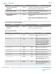
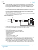
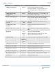
Figure 3-3: fPLL Block Diagram
VCO
PFD
Up
Down
Delta Sigma
Modulator
L Counter
/1, 2, 4, 8
N Counter
M Counter
Charge
Pump and
Loop Filter
C Counter
Refclk
Multiplexer
Reference Clock Network
Receiver Input Pin
Output of Another PLL with PLL Cascading
Dedicated Reference Clock Pin
Global Clock or Core Clock
refclk
Input
Reference
Clock
fbclk
/2
/2
The fPLL generates output clocks with a fixed frequency and phase relation to an input reference clock. In
the fractional frequency mode, the fPLL supports data rates from 1 Gbps to 12.5 Gbps.
Input Reference Clock
This is the dedicated input reference clock source for the PLL.
The input reference clock can be sourced from one of the following:
• Dedicated reference clock pin
• Reference clock network
• Receiver input pin
• Output of another PLL with PLL cascading
• Global clock or the core clock network
The input reference clock is a differential signal. Altera recommends using the dedicated reference clock
pin as the input reference clock source for best jitter performance. The input reference clock must be
stable and free-running at device power-up for proper PLL operation. If the reference clock is not
available at device power-up, then you must recalibrate the PLL when the reference clock is available.
Note:
The ATX fPLL calibration is clocked by the CLKUSR clock, which must be stable and available for
the calibration to proceed. Refer to the Calibration section for details about PLL calibration and
CLKUSR clock.
UG-01143
2015.05.11
fPLL
3-13
PLLs and Clock Networks
Altera Corporation
Send Feedback