
User guide
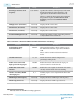
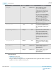
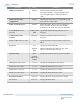

Port Direction Clock Domain Description
mcgb_rst Input Asynchronous Master CGB reset control.
If you use PLL feedback
compensation bonding mode,
deassert this reset at the same
time as pll_powerdown .
If you do not use PLL feedback
compensation bonding, then you
can deassert this port after pll_
powerdown is deasserted, but
before tx_analogreset is
deasserted. Alternatively, you
can deassert this port at the same
time as pll_powerdown .
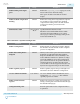
mcgb_aux_clk0 Input N/A Used for PCIe implementation
to switch between fPLL and ATX
PLL during link speed negotia‐
tion.
tx_bonding_clocks[5:0] Output N/A Optional 6-bit bus which carries
the low speed parallel clock
outputs from the master CGB.
Each transceiver channel in a
bonded group has this 6-bit bus.
Used for channel bonding, and
represents the x6/xN clock
network.
mcgb_serial_clk Output N/A High speed serial clock output
for x6/xN non-bonded configu‐
rations.
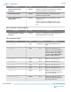
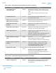
pcie_sw[1:0] Input Asynchronous 2-bit rate switch control input
used for PCIe protocol
implementation.
pcie_sw_done[1:0] Output Asynchronous 2-bit rate switch status output
used for PCIe protocol
implementation.
Related Information
• Calibration on page 1-24
• Avalon Interface Specifications
The ports related to reconfiguration are compliant with the Avalon specification. Refer to the Avalon
specification for more details about these ports.
3-12
ATX PLL IP Core
UG-01143
2015.05.11
Altera Corporation
PLLs and Clock Networks
Send Feedback