
User guide

as a starting point. Or, you can use the protocol presets described in Presets. You can then modify the
settings to meet your specific requirements.
• Ensure that the data rate is between 17400 and 28100 Mbps. Select a CDR reference clock to match
your data rate.
• Set the Enhanced PCS / PMA interface width to 64 bits.
• Set the FPGA Fabric / Enhanced PCS interface width to 64 bits.
• You can enable RX/TX FIFO double width mode to create a FPGA fabric / PCS interface width of
128 bits.
• Click Finish to generate the Native PHY IP (this is your RTL file).
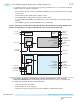
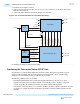
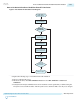
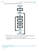
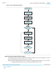
Figure 2-140: Signals and Ports of the Native PHY for Basic (Enhanced PCS) Transceiver Configuration
Rule for Data Rates Above 17.4 Gbps and FPGA Fabric / PCS Interface width of 128 bits
Reconfiguration
Registers
NIOS
Hard Calibration IP
TX PMA
Serializer
tx_serial_data
tx_serial_clk0
(from TX PLL)
rx_cal_busy
tx_cal_busy
rx_serial_data
rx_control[19:0]
rx_cdr_refclk0
rx_is_lockedtodata
rx_is_lockedtoref
rx_parallel_data[127:0]
tx_control[17:0] tx_control[17:0]
tx_digital_resettx_digital_reset
tx_parallel_data[127:0]
reconfig_clk
reconfig_avmm
reconfig_reset
tx_coreclkin
tx_clkout
tx_enh_data_valid
tx_parallel_data[127:0]
tx_coreclkin
tx_clkout
tx_enh_data_valid
RX PMA
TX Enhanced PCS
RX Enhanced PCS
Deserializer
refclk
CDR
rx_clkout
rx_coreclkin
rx_clkout
rx_coreclkin
rx_analog_reset
tx_analog_reset
rx_digital_resetrx_digital_reset
rx_parallel_data[127:0]
rx_control[19:0]
4. Select Tools > IP Catalog > Basic Functions > Clocks > PLLs and Resets > PLL > Arria 10
Transceiver ATX PLL. Refer to Instantiating the ATX PLL IP Core on page 3-5 for detailed steps.
5. Configure the ATX PLL IP using the Parameter Editor.
• Select the GT clock output buffer.
• Enable the PLL GT clock output port.
• Set the PLL output clock frequency to the Native PHY IP recommended frequency.
2-320
How to Implement Designs for Data Rates Above 17.4 Gbps Using Enhanced...
UG-01143
2015.05.11
Altera Corporation
Implementing Protocols in Arria 10 Transceivers
Send Feedback