
User guide
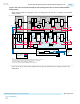
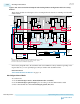
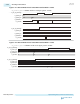
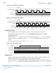
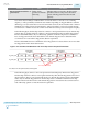

Figure 2-108: Transceiver Channel Datapath and Clocking for the Basic and Basic with Rate Match
Configurations
The clocking calculations in this figure are for an example when the data rate is 1250 Mbps and the PMA
width is 10 bits.
RX
FIFO
Byte
Deserializer
8B/10B Decoder
Rate Match FIFO (3)
Receiver PMA
Word Aligner
Deserializer
CDR
Receiver Standard PCS
Transmitter Standard PCS
Transmitter PMA
Serializer
tx_serial_data
rx_serial_data
FPGA
Fabric
TX
FIFO
Byte Serializer
8B/10B Encoder
PRBS
Generator
TX Bit Slip
/2
/2
Parallel Clock
Serial Clock
Parallel and Serial Clock
Parallel and Serial Clock
Clock Divider
rx_pma_div_clkout
Serial Clock
Clock Generation Block (CGB)
ATX PLL
CMU PLL
fPLL
tx_coreclkin
rx_coreclkin
rx_clkout or
tx_clkout
Parallel Clock
(Recovered)
Parallel Clock
(From Clock
Divider)
tx_clkout
tx_clkout
tx_clkout
rx_clkout
PRBS
Verifier
tx_pma_div_clkout
16
16
10
10
125 MHz (1)
Notes:
1. The parallel clock (tx_clkout or rx_clkout) is calculated as data rate/PCS-PMA interface width =1250/10 = 125 MHz.
When the Byte Serializer is set to Serialize x2 mode, tx_clkout and rx_clkout become 1250/20 = 62.5 MHz.
2. The serial clock is calculated as data rate/2. The PMA runs on a dual data rate clock.
3. This block is only enabled when using the Basic with Rate Match transceiver configuration rule.
125 MHz (1)
62.5 MHz (1)
62.5 MHz (1)
625 MHz (2)
In low latency mode, much of the Standard PCS is bypassed, which allows more design control in the
FPGA fabric.
UG-01143
2015.05.11
Using the Basic/Custom, Basic/Custom with Rate Match Configurations of...
2-291
Implementing Protocols in Arria 10 Transceivers
Altera Corporation
Send Feedback