
User guide
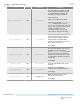
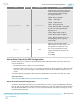
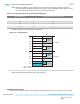
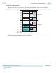
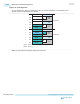
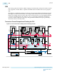

Figure 2-94: x4 Alternate Configuration
The figure below shows an alternate way of placing 4 bonded channels. In this case, the logical PCS
Master Channel number must be specified as channel 4.
CH5
CH4
CH3
CH2
CH1
CH0
CH5
CH4
CH3
CH2
CH1
CH0
Master CH
fPLL
ATX
PLL
fPLL
ATX
PLL
fPLL
ATX
PLL
fPLL
ATX
PLL
Logical
Channel
Physical
Channel
0
1
Transceiver bank
2
3
Data CH
Data CH
Data CH
Master
CGB
Master
CGB
Master
CGB
Master
CGB
Transceiver bank
As indicated in the figures above, the fitter picks either physical CH1 or CH4 as the PCS master in bonded
configurations for PIPE.
PHY IP Core for PCIe (PIPE) Link Equalization for Gen3 Data Rate
Gen3 mode requires TX and RX link equalization because of the data rate, the channel characteristics,
receiver design, and process variations. The link equalization process allows the Endpoint and Root Port
to adjust the TX and RX setup of each lane to improve signal quality. This process results in Gen3 links
with a receiver Bit Error Rate (BER) that is less than 10
-12
.
For detailed information about the four-stage link equalization procedure for 8.0 GT/s data rate, refer to
Section 4.2.3 in the PCI Express Base Specification, Rev 3.0. A new LTSSM state, Recovery.Equalization
with Phases 0–3, reflects progress through Gen3 equalization. Phases 2 and 3 of link equalization are
optional. Each link must progress through all four phases, even if no adjustments occur. If you skip Phases
2 and 3, you will speed up link training at the expense of link BER optimization.
UG-01143
2015.05.11
PHY IP Core for PCIe (PIPE) Link Equalization for Gen3 Data Rate
2-265
Implementing Protocols in Arria 10 Transceivers
Altera Corporation
Send Feedback