
User guide
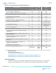

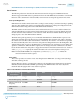


PCIe Gen3 Capability
Mode Enabled
Gen1 Gen2 Gen3
pipe_rate [1:0] 2'b00 2'b01 2'b1x
Figure 2-79: Rate Switch Change
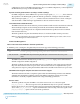
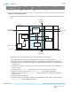
The block-level diagram below shows a high level connectivity between ASN and Standard PCS and Gen3
PCS.
PHYSTATUS
GEN
PHYSTATUS
GEN
TX
FIFO
Gen3 ASN
(Gen1, Gen2, Gen3)
PCS/PMA INF Gen3 PCS
pipe_rate[1:0]
from FPGA Fabric
Control Plane
Bonding Up
Control Plane
Bonding Down
pipe_sw
pipe_sw_done
pipe_phy_status
pll_pcie_clk
PMA
Standard PCS
/2
(for Gen1 Only)
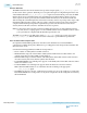
The sequence of speed change between Gen1, Gen2, and Gen3 occurs as follows:
1. The PHY-MAC layer implemented in FPGA Fabric requests a rate change through pipe_rate[1:0].
2. The ASN block waits for the TX FIFO to flush out data. Then the ASN block asserts the PCS reset.
3. The ASN asserts the clock shutdown signal to the Standard PCS and Gen3 PCS to dynamically shut
down the clock.
4. When the rate changes to or from the Gen3 speed, the ASN asserts the clock and data multiplexer
selection signals.
5. The ASN uses a pipe_sw[1:0] output signal to send a rate change request to the PMA.
6. The ASN continuously monitors the pipe_sw_done[1:0] input signal from the PMA.
7. After the ASN receives the pipe_sw_done[1:0] signal, it deasserts the clock shut down signals to
release the clock.
8. The ASN deasserts the PCS reset.
9. The ASN sends the speed change completion to the PHY-MAC interface. This is done through the
pipe_phy_status signal to PHY-MAC interface.
2-236
Rate Switch
UG-01143
2015.05.11
Altera Corporation
Implementing Protocols in Arria 10 Transceivers
Send Feedback