
User guide


Each transceiver bank includes six transceiver channels in all devices except for the devices with 66
transceiver channels. These devices (with 66 transceiver channels) have both six channel and three
channel transceiver banks. The uppermost transceiver bank on the left and the right side of these devices
is a three channel transceiver bank. All other devices contain only six channel transceiver banks.
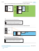
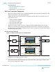
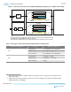
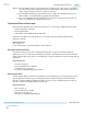
The figures below show the transceiver bank architecture with the phase locked loop (PLL) and clock
generation block (CGB) resources available in each bank.
Figure 1-14: Three-Channel GX Transceiver Bank Architecture
PMA
Channel PLL
(CDR Only)
PCS
Local CGB2
CH2
PMA
Channel PLL
(CMU/CDR)
PCS
Local CGB1
CH1
PMA
Channel PLL
(CDR Only)
PCS
Local CGB0
CH0
FPGA Core
Fabric
Three-Channel GX Transceiver Bank
Master
CGB0
fPLL0
ATX
PLL0
Clock
Distribution
Network
Note: This figure is a high level overview of the transceiver bank architecture. For details about the
available clock networks refer to the PLLs and Clock Networks chapter.
UG-01143
2015.05.11
Transceiver Bank Architecture
1-17
Arria 10 Transceiver PHY Overview
Altera Corporation
Send Feedback