
User guide
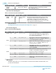
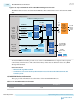
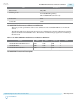
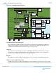

Table 2-116: PMA Registers
Address Bit R/W Name Description
0x444
1 RW reset_tx_digital Writing a 1 asserts the internal TX digital reset
signal. You must write a 0 to clear the reset
condition.
2 RW reset_rx_analog Writing a 1 causes the internal RX analog reset
signal to be asserted. You must write a 0 to clear
the reset condition.
3 RW reset_rx_digital Writing a 1 causes the internal RX digital reset
signal to be asserted. You must write a 0 to clear
the reset condition.
0x461 0 RW phy_serial_
loopback
Writing a 1 puts the channel in serial loopback
mode.
0x464 0 RW pma_rx_set_
locktodata
When set, programs the RX clock data recovery
(CDR) PLL to lock to the incoming data.
0x465 0 RW pma_rx_set_
locktoref
When set, programs the RX CDR PLL to lock to
the reference clock.
0x466 0 RO pma_rx_is_
lockedtodata
When asserted, indicates that the RX CDR PLL is
locked to the RX data, and that the RX CDR has
changed from LTR to LTD mode.
0x467 0 RO pma_rx_is_
lockedtoref
When asserted, indicates that the RX CDR PLL is
locked to the reference clock.
Creating a 10GBASE-KR Design
Follow these steps to create a 10GBASE-KR design.
1. Generate the 10GBASE-KR PHY with the required parameterization.
The 10GBASE-KR PHY IP core includes a reconfiguration block. The reconfiguration block provides
the Avalon-MM interface to access the PHY registers.
2. Instantiate a reset controller. You can generate an Altera Transceiver Reset Controller IP core from the
IP Catalog. You must connect the Transceiver Reset Controller IP core and 10GBASE-KR PHY IP core
power and reset signals.
3. Instantiate one TX PLL for the 1G data rate and one TX PLL for the 10G data rate. Connect the high
speed serial clock and PLL lock signals between 10GBASE-KR PHY and TX PLLs. For the 1G data rate
you can use either fPLL, or ATX, or CMU PLL. For the 10G data rate you can use ATX PLL or CMU
PLL.
4. Generate a fractional PLL to create the 156.25 MHz XGMII clock from the 10G reference clock.
5. Use the tx_pma_divclk from the 10GBASE-KR PHY or generate a fPLL to create the 156.25 MHz
XGMII clock from the 10G reference clock.
Unlike in the 10GBASE-KR PHY IP core for Stratix V devices, no Memory Initialization Files (.mif)
are required for the 10GBASE-KR design in Arria 10 devices.
6. Complete the design by creating a top level module to connect all the IP (10GBASE-KR PHY IP core,
PLL IP core, and Reset Controller) blocks.
UG-01143
2015.05.11
Creating a 10GBASE-KR Design
2-161
Implementing Protocols in Arria 10 Transceivers
Altera Corporation
Send Feedback