
User guide


network. In feedback compensation bonding, the separate x6 clocks are in phase and frequency aligned
with each other. One PLL from each transceiver bank drives the clock to master CGB. The CGB then
drives these clocks to the TX channels that reside in the same bank only. In xN bonding, all channels are
driven by the xN clock network. The data rate decrease imposed by xN bonding does not apply to PLL
feedback compensation bonding.
The feedback to the PLL for each bonded group is the parallel clock from the master CGB, which has the
same frequency as tx_clkout. The reference clock for the PLL must match the frequency of this feedback
clock. For example, given that the Interlaken interface runs at 12.5 Gbps per lane, and PCS-PMA width is
40 bits, the only available frequency of the reference clock is 312.5 MHz.
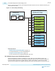
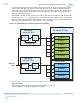
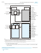
Figure 2-16: 10X12.5 Gbps PLL Feedback Compensation Bonding
Transceiver PLL
Instance (6.25 GHz)
ATX PLL
Master
CGB
x6
Feedback Clock
Reference
Clock
TX Channel
TX Channel
TX Channel
TX Channel
TX Channel
TX Channel
TX Channel
Transceiver Bank 2
TX Channel
TX Channel
TX Channel
Transceiver Bank 1
Native PHY Instance
(10 Ch Bonded 12.5 Gbps)
Transceiver PLL
Instance (6.25 GHz)
ATX PLL
Master
CGB
Feedback Clock
x6
Related Information
Implementing PLL Feedback Compensation Bonding Mode on page 3-55
For other limitations on feedback compensation bonding
UG-01143
2015.05.11
PLL Feedback Compensation Clock Bonding Scenario
2-81
Implementing Protocols in Arria 10 Transceivers
Altera Corporation
Send Feedback