
User guide
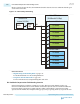


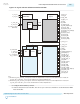

Because of xN clock network skew, the maximum achievable data rate decreases when TX channels span
several transceiver banks.
Figure 2-15: 10X12.5 Gbps xN Bonding
Transceiver PLL
Instance (6.25 GHz)
ATX PLL
Native PHY Instance
(10 Ch Bonded 12.5 Gbps)
TX Channel
TX Channel
TX Channel
TX Channel
TX Channel
TX Channel
TX Channel
Transceiver Bank 2
TX Channel
TX Channel
TX Channel
Master
CGB
xN
Transceiver Bank 1
Related Information
• Implementing x6/xN Bonding Mode on page 3-54
For detailed information on xN bonding limitations
• Using PLLs and Clock Networks on page 3-49
For more information about implementing PLLs and clocks
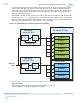
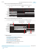
PLL Feedback Compensation Clock Bonding Scenario
In the following figure, each lane is running at 12.5 Gbps. The first six TX channels reside in one
transceiver bank and the other four TX channels reside in the adjacent transceiver bank. The difference
between feedback compensation bonding and xN bonding is that feedback compensation bonding
separates the TX channels into multiple bonding groups, each group being driven by a separate x6 clock
2-80
PLL Feedback Compensation Clock Bonding Scenario
UG-01143
2015.05.11
Altera Corporation
Implementing Protocols in Arria 10 Transceivers
Send Feedback