
User guide

Chapter 6: PHY IP Core for PCI Express (PIPE) 6–15
Interfaces
March 2012 Altera Corporation Altera Transceiver PHY IP Core
User Guide
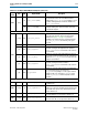
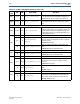
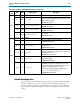
0x042 [1:0]
W
reset_control
(write)
Writing a 1 to bit 0 initiates a TX digital reset using the
reset controller module. The reset affects channels
enabled in the reset_ch_bitmask. Writing a 1 to bit
1 initiates a RX digital reset of channels enabled in the
reset_ch_bitmask.
R
reset_status
(read)
Reading bit 0 returns the status of the reset controller TX
ready bit. Reading bit 1 returns the status of the reset
controller RX ready bit.
Reset Controls –Manual Mode
0x044
[31:0] RW
reset_fine_control
You can use the
reset_fine_control
register to create
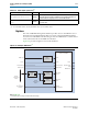
your own reset sequence. The reset control module,
illustrated in Figure 1–1 on page 1–2, performs a
standard reset sequence at power on and whenever the
phy_mgmt_clk_reset
is asserted. Bits [31:4, 0] are
reserved.
[31:4] RW
Reserved
It is safe to write 0s to reserved bits.
[3] RW
reset_rx_digital
Writing a 1 causes the RX digital reset signal to be
asserted, resetting the RX digital channels enabled in
reset_ch_bitmask. You must write a 0 to clear the
reset condition.
[2] RW
reset_rx_analog
Writing a 1 causes the internal RX digital reset signal to
be asserted, resetting the RX analog logic of all channels
enabled in reset_ch_bitmask. You must write a 0 to
clear the reset condition.
[1] RW
reset_tx_digital
Writing a 1 causes the internal TX digital reset signal to be
asserted, resetting all channels enabled in
reset_ch_bitmask. You must write a 0 to clear the
reset condition.
[0] RW
pll_powerdown
Writing a 1 causes the internal TX PLL to powerdown. If
you reset the transceiver, you must assert
pll_powerdown
by writing a 1 to this register and then
writing a 0 after 1 μs. Asserting
pll_powerdown
also
asserts
tx_analogreset
which is required for Gen2
operation.
PMA Control and Status Registers
0x061 [31:0] RW
phy
_
serial
_
loopback
Writing a 1 to channel <
n
> puts channel <
n
> in serial
loopback mode.
0x063 [31:0] R
pma_rx_signaldetect
When channel <n> =1, indicates that receive circuit for
channel <n> senses the specified voltage exists at the RX
input buffer. This option is only operational for the PCI
Express PHY IP core.
0x064 [31:0] RW
pma_rx_set_locktodata
When set, programs the RX CDR PLL to lock to the
incoming data. Bit <n> corresponds to channel <n>.
0x065 [31:0] RW
pma_rx_set_locktoref
When set, programs the RX CDR PLL to lock to the
reference clock. Bit <n> corresponds to channel <n>.
Table 6–12. PCI Express PHY (PIPE) IP Core Registers (Part 2 of 4)
Word
Addr
Bits R/W Register Name Description