
User guide

9–24 Chapter 9: Deterministic Latency PHY IP Core
Simulation Files and Example Testbench
Altera Transceiver PHY IP Core March 2012 Altera Corporation
User Guide
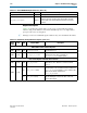
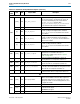
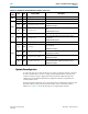
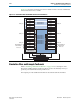
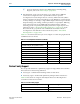
Figure 9–5 shows the placement of transceiver banks in Arria V devices and indicates
the channels that are not available.
Simulation Files and Example Testbench
Refer to “Running a Simulation Testbench” on page 1–4 for a description of the
directories and files that the Quartus II software creates automatically when you
generate your Deterministic Latency PHY IP core.
This chapter provides additional information about the document and Altera.
Figure 9–5. Channel Placement and Available Channels in Arria V Devices
GXB_R0
GXB_R1
GXB_L0
GXB_L1
GXB_R2GXB_L2
Devices Available
Number of Channels Per Bank
Transceiver Bank Names
5AGXB5KF40
5AGXB7KF40
5AGXA5HF35
5AGXA7HF35
5AGXB1HF35
5AGXB1HF40
5AGXB3HF35
5AGXB3HF40
5AGXB5HF35
5AGXB7HF35
5AGXA1EF31
5AGXA3EF31
PCIe Hard IP
PCIe Hard IP
Ch 5
Ch 4
Ch 3
Ch 2
Ch 1
Ch 0
Ch 0
Ch 1
Ch 2
Ch 3
Ch 4
Ch 5
Ch 5
Ch 4
Ch 3
Ch 2
Ch 1
Ch 0
Ch 0
Ch 1
Ch 2
Ch 3
Ch 4
Ch 5
Ch 5
Ch 4
Ch 3
Ch 2
Ch 1
Ch 0
Ch 0
Ch 1
Ch 2
Ch 3
Ch 4
Ch 5
Not Available for
Deterministic
Protocols
Not Available for
Deterministic
Protocols