
User guide


8–16 Chapter 8: Low Latency PHY IP Core
Interfaces
Altera Transceiver PHY IP Core March 2012 Altera Corporation
User Guide
f For more information about the Avalon-MM and Avalon-ST protocols, including
timing diagrams, refer to the Avalon Interface Specifications.
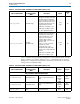
Register Descriptions
Table 8–15 describes the registers that you can access over the PHY Management
Interface using word addresses and a 32-bit embedded processor.
1 Writing to reserved or undefined register addresses may have undefined side effects.
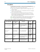
phy_mgmt_write
Input Write signal.
phy_mgmt_read
Input Read signal.
Table 8–14. Avalon-MM PHY Management Interface (Part 2 of 2)
Signal Name Direction Description
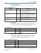
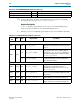
Table 8–15. Low Latency PHY IP Core Registers (Part 1 of 2)
Word
Addr
Bits R/W Register Name Description
Reset Control Registers–Automatic Reset Controller
0x041 [31:0] RW
reset_ch_bitmask
Reset controller channel bitmask for digital resets. The
default value is all 1s. Channel <
n
> can be reset when
bit<
n
> = 1.
0x042 [1:0]
W
reset_control
(write)
Writing a 1 to bit 0 initiates a TX digital reset using the
reset controller module. The reset affects channels
enabled in the reset_ch_bitmask. Writing a 1 to
bit 1 initiates a RX digital reset of channels enabled in
the reset_ch_bitmask.
R
reset_status
(read)
Reading bit 0 returns the status of the reset controller
TX ready bit. Reading bit 1 returns the status of the
reset controller RX ready bit.
PMA Control and Status Registers
0x061 [31:0] RW
phy
_
serial
_
loopback
Writing a 1 to channel <
n
> puts channel <
n
> in serial
loopback mode. For information about pre- or
post-CDRserial loopback modes, refer to “Loopback
Modes” on page 10–39 .
0x063 [31:0] R
pma_rx_signaldetect
When channel <n> =1, indicates that receive circuit for
channel <n> senses the specified voltage exists at the
RX input buffer.
0x064 [31:0] RW
pma_rx_set_locktodata
When set, programs the RX CDR PLL to lock to the
incoming data. Bit <n> corresponds to channel <n>.
0x065 [31:0] RW
pma_rx_set_locktoref
When set, programs the RX CDR PLL to lock to the
reference clock. Bit <n> corresponds to channel <n>.