
User guide

8–6 Chapter 8: Low Latency PHY IP Core
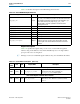
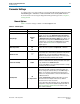
Parameter Settings
Altera Transceiver PHY IP Core March 2012 Altera Corporation
User Guide
PLL Reconfiguration Options
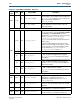
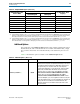
Table 8–5 describes the options available on the PLL Reconfiguration tab. For more
information about transceiver reconfiguration registers, refer to “PLL
Reconfiguration” on page 10–18.
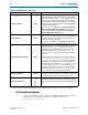
Enable rx_coreclkin
(1)
On/Off
When you turn this option on,
rx_coreclkin
connects to the read
clock of the RX phase compensation FIFO and you can clock the
parallel RX output data using
rx_coreclk
. This port allows you to
clock the read side of the RX phase compensation FIFO with a
user-provided clock, either the FPGA fabric clock, the FPGA fabric
RX interface clock, or the input reference clock. rx_coreclkin is not
available for the GT datapath.
You must turn this option On when the FPGA fabric transceiver
interface width:PCS-PMA Interface width is 50:40 or when you
specify the 10G datapath with a fabric transceiver interface
width:PCS-PMA Interface width of 64:32.
Enable TX bitslip On/Off
When you turn this option on, the variant includes the
tx_bitslip
signal. For every rising edge of the
tx_bitslip
signal, the word
boundary is shifted by 1 bit. Each bit slip removes the earliest
received bit from the received data.
This option is only available for the Standard and 10G datapath.
Enable embedded reset control On/Off
This option is turned on by default. When On, the embedded reset
controller initiates the reset sequence when it receives a positive
edge on the
phy_mgmt_clk_reset
input signal. For more
information about the embedded reset controller, refer to the
“Embedded Reset Controller” section in the Transceiver Reset
Control in Stratix V Devices in volume 3 of the Stratix V Device
Handbook.
Disable this option to implement your own reset sequence using
the
tx_analogreset
,
rx_analogreset
,
tx_digitalreset
,
rx_digitalreset
, and
pll_powerdown
which are available as
top-level ports of the Low Latency Transceiver PHY. When you
design your own reset controller, the
tx_ready
and
rx_ready
are
not top-level signals of the core. For more information about
designing a reset controller, refer to the “User-Controller Reset
Controller” section in the Transceiver Reset Control in Stratix V
Devices in volume 3 of the Stratix V Device Handbook.
Avalon data interfaces On/Off
When you turn this option On, the order of symbols is changed.
This option is typically required if you are planning to import your
Low Latency Transceiver PHY IP core into a Qsys system.
Avalon data symbol size
All bits
8
10
16
20
Specifies the number of bits that are in the smallest unit of data.
One or more symbols make up a single unit of data transferred in a
cycle.
Note to Table 8–5:
(1) For more information refer to the “FPGA Fabric-Transceiver Interface Clocking” section in the Stratix V Transceiver Clocking chapter.
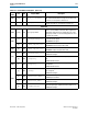
Table 8–5. Additional Options (Part 2 of 2)
Name Value Description