
User guide

Chapter 8: Low Latency PHY IP Core 8–5
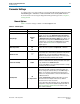
Parameter Settings
March 2012 Altera Corporation Altera Transceiver PHY IP Core
User Guide
Additional Options
The parameters on the Additional Options tab control clocking and datapath options.
Both bonded (×N) and non-bonded modes are available. In bonded modes, a single
PLL can drive all channels. In non-bonded modes, each channel may have its own
PLL.
Table 8–5 describes the options available on the Additional Options tab.
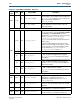
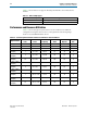
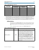
16 8 or 16 — data rate/16
20 10 or 20 — data rate/20
32 16 32 data rate/32
40 20 40 data rate/40
50 — 40 data rate/50
(1)
64 — 32 data rate/32
(2)
64 — 64 data rate/64
66 — 40 data rate/66
Note to Table 8–4:
(1) For this datapath configuration, the
tx_clkout
frequency generated by the the Low Latency PHY is the data rate /40. You must generate a /50
frequency clock from the /40 clock and feed this clock back into the
tx_coreclkin
. The
rx_clkout
frequency generated by the Low Latency
PHY is /40 of the data rate. You must generate a /50 frequency from the recovered clock and feed this back into the
rx_coreclkin
.
(2) For this datapath configuration, the
tx_clkout
frequency generated by the the Low Latency PHY is the data rate/32. You must generate a /64
frequency clock from the /32 clock and feed this clock back into the
tx_coreclkin
. The
rx_clkout
frequency generated by the Low Latency
PHY is the data rate/32. You must generate a /64 frequency from the recovered clock and feed this back into the
rx_coreclkin.
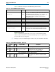
Table 8–4. Datapath Width Support (Part 2 of 2)
FPGA Fabric-Transceiver
Interface Width
PCS-PMA Interface Width
tx_clkout and rx_clkout
frequency
Standard Datapath 10G Datapath
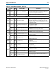
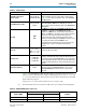
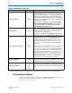
Table 8–5. Additional Options (Part 1 of 2)
Name Value Description
Enable tx_coreclkin
(1)
On/Off
When you turn this option on,
tx_coreclkin
connects to the
write clock of the TX phase compensation FIFO and you can clock
the parallel TX data generated in the FPGA fabric using this port.
This port allows you to clock the write side of the TX phase
compensation FIFO with a user-provided clock, either the FPGA
fabric clock, the FPGA fabric-TX interface clock, or the input
reference clock. You must turn this option On when the FPGA
fabric transceiver interface width:PCS-PMA Interface width is
50:40 or when you specify the 10G datapath with a fabric
transceiver interface width:PCS-PMA Interface width of 64:32.
For the GT datapath, if you are using different reference clock pins
for the TX and RX channels, you must instantiate two separate Low
Latency PHY IP core instances for TX and RX channels. The
reference clock pins for each channel must reside in the same
transceiver bank.