
User guide

8–4 Chapter 8: Low Latency PHY IP Core
Parameter Settings
Altera Transceiver PHY IP Core March 2012 Altera Corporation
User Guide
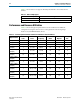
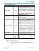
Table 8–4 lists Standard and 10G datapath widths for the FPGA fabric-transceiver
interface, the PCS-PMA interface, and the resulting frequencies for the
tx_clkout
and
rx_clkout
parallel clocks. In almost all cases, the parallel clock frequency is described
by the following equation:
frequency
parallel clock
= data rate/FPGA fabric-transceiver interface width
1 The FPGA fabric-transceiver interface width is always 128 bits for the GT datapath.
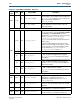
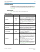
FPGA fabric transceiver
interface width
8, 10, 16, 20, 32,
40, 50, 64, 66, 128
This option indicates the parallel data fabric transceiver interface
width. GT datapath supports a single width of 128 bits. Refer
toTable 8–4 for the supported interface widths of the Standard
and 10G datapaths.
PCS-PMA interface width
8, 10, 16, 20, 32,
30, 64
The PCS-PMA interface width depends on the FPGA fabric
transceiver interface width and the Datapath type. Refer to
Table 8–4 for the supported interface widths of the Standard and
10G datapaths.
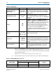
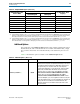
PLL type
CMU
ATX
The CMU PLL is available for the Standard and 10G datapaths.
The ATX PLL. is available for the S
tandard, 10G, and GT
datapaths. The CMU PLL has a larger frequency range than the
ATX PLL. The ATX PLL is designed to improve jitter performance
and achieves lower channel-to-channel skew; however, it
supports a narrower range of data rates and reference clock
frequencies. Another advantage of the ATX PLL is that it does not
use a transceiver channel, while the CMU PLL does.
An informational message displays in the message panel if the
PLL type that you select is not available at the frequency
specified.
Data rate
Standard:
1–8.5 Gbps
10G:
1–12.5 Gbps
GT:
20–28 Gbps
Specifies the data rate in Mbps.
Base data rate
1 × Lane rate
2 × Lane rate
4 × Lane rate
Select a base data rate that minimizes the number of PLLs
required to generate all the clocks required for data transmission.
By selecting an appropriate base data rate, you can change data
rates by changing the divider used by the clock generation block.
For higher frequency data rates 2 × and 4× base data rates are not
available.
Input clock frequency Variable
Specifies the frequency of the PLL input reference clock. The
frequency required is the Base data r ate/2. You can use any
Input clock frequency that allows the PLLs to generate this
frequency.
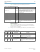
Table 8–3. General Options
Name Value Description
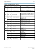
Table 8–4. Datapath Width Support (Part 1 of 2)
FPGA Fabric-Transceiver
Interface Width
PCS-PMA Interface Width
tx_clkout and rx_clkout
frequency
Standard Datapath 10G Datapath
8 8 — data rate/8
10 10 — data rate/10