
User guide

Chapter 7: Custom PHY IP Core 7–9
Parameter Settings
March 2012 Altera Corporation Altera Transceiver PHY IP Core
User Guide
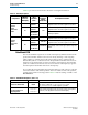
PLL Reconfiguration
Table 7–10 lists the PLL Reconfigurations options. For more information about
transceiver reconfiguration registers, refer to “PLL Reconfiguration” on page 10–18.
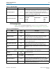
Byte ordering pattern
11111011
Specifies the pattern that identifies the SOP.
For 16-bit byte ordering pattern you must include a 2-bit pad so that
the pattern entered is in the following format: 00 <pattern> 00
<pattern>. For example, if the required pattern is 10111100, enter the
following pattern: 00101111000010111100
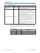
Byte ordering pad pattern
00000000
Specifies the pad pattern that is inserted to align the SOP. Enter the
following size pad patterns:
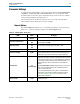
Data Width 8B/10B Encoded? Pad Pattern
8, 16, 32 No 8 bits
10,20,40 No 10 bits
8, 16, 32 Yes 9 bits
Table 7–9. Byte Order Options
Name Value Description
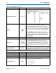
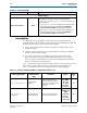
Table 7–10. PLL Reconfigurations
Name Value Description
Allow PLL Reconfiguration On/Off
You must enable this option if you plan to reconfigure the PLLs in
your design. This option is also required to simulate PLL
reconfiguration.
Number of TX PLLs 1–4
Specifies the number of TX PLLs required for this instance of the
Custom PHY. More than 1 PLL may be required if your design
reconfigures channels to run at multiple frequencies.
Number of input clocks 1–5
Specifies the number of input reference clocks. More than one
reference clock may be required if your design reconfigures channels
to run at multiple frequencies.
Main TX PLL logical index 0–3
Specifies the index for the TX PLL that should be instantiated at
startup. Logical index 0 corresponds to TX PLL0, and so on.
Main TX PLL input clock
source
0–3
Specifies the index for the TX PLL input clock that should be
instantiated at startup. Logical index 0 corresponds to input clock 0
and so on.
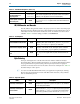
TX PLL (0–3)
(Refer to Table 7–3 on page 7–3 for a detailed explanation of these parameters.)
PLL Type
CMU
ATX
Specifies the PLL type.
Base data rate
1 × Lane rate
2 × Lane rate
4 × Lane rate
Specifies Base data rate.
Input clock frequency Variable
Specifies the frequency of the PLL input reference clock. The
frequency required is the Base data rate/2. You can use any Input
clock frequency that allows the PLLs to generate this frequency.
Selected input clock source 0–4
Specifies the index of the input clock for this TX PLL. Logical index 0
corresponds to input clock 0 and so on.