
User guide

A–6 Appendix A: Programming the Flash Device
Restoring the Factory Design to the Flash Device
Cyclone III FPGA Development Kit User Guide September 2010 Altera Corporation
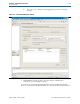
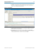
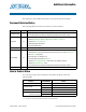
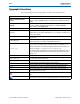
11. Turn on Page_0 and OPTION_BITS options in the Program/Configure column
that correspond to the CFI_512MB device (Figure A–3). This results in writes only
to the flash page zero and the option bit register.
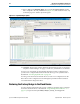
12. Click Start. The message window details the flash writing progress to successful
completion. Flash writing to one page, as in this case, can take five to six minutes.
You have now successfully programmed the flash device with a configuration for
your board. To configure the board from the flash device, power cycle the board as
described in “Powering Up the Board” on page 4–2.
Powering on the board causes the flash device to load a new configuration into the
FPGA device. The Configuration Done LED lights up and the hardware functions
associated with the design take effect.
Restoring the Factory Design to the Flash Device
To restore the development board to factory conditions, repeat the steps for writing a
new POF to the flash device as described in “Programming the Flash Device” on
page A–4, except select the cycloneIII_3c120_dev_factory_recovery.pof file.
Figure A–3. Program/Configure Options