
User guide


Chapter 7: Power Measurement 7–3
Measuring Power
September 2010 Altera Corporation Cyclone III FPGA Development Kit User Guide
Measuring Power
You can measure power by using the analog-to-digital (A/D) circuitry on the
development board or by using a digital multi-meter (DMM) across on-board sense
resistors. However, note that, depending on the DMM accuracy, the on-board A/D
measurements tend to produce considerably more accurate results.
A/D Measurements
The POWER SELECT rotary switch SW4 sets the development board to measure and
display FPGA core power or I/O output power (Table 7–4).
Measuring V
CC_INT
Power
To measure FPGA core power at V
CC_INT
= 1.2 V for various power states, perform the
following steps:
1. Ensure that the 8-position SW1 DIP switch is configured to the default settings
shown in Table 4–1 on page 4–2.
2. Download the cycloneIII_3c120_dev_power_demo.sof file as described in
“Configuring the FPGA” on page 4–4. You can find the power design example in
<path>\...\examples\cycloneIII_3c120_dev_power_demo.
3. Set the POWER SELECT rotary switch SW4 to 0 to measure the internal V
CC_INT
power in watts.
4. Observe the power on the 4-digit hexadecimal power display.
The on-board power measurements are performed at a high rate. For this reason, it
appears that the display is dithering; however, what is actually taking place is the
very fast momentary changes on the power rail.
5. Using the user input push buttons (Table 7–1 on page 7–1), advance through the
power states in Table 7–2 and Table 7–3 on page 7–2. Notice how power increases
as frequency and resources increase.
f For information about measuring power sources, refer to the Cyclone III 3C120
Development Board Reference Manual.
Measuring I/O Power
This example uses FPGA I/O banks 1, 2, 5, and 6. Using the SW4 settings (Table 7–4),
measure the power for I/O banks 1 and 2, then for I/O banks 5 and 6, by performing
the following steps:
1. Ensure that the 8-position SW1 DIP switch is configured to the default settings
shown in Table 4–1 on page 4–2.
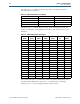
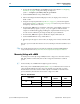
Table 7–4. Switch SW4 Power Selection
Switch Position FPGA Power I/O Banks
0 Core: V
CC_INT
, 1.2 V —
5 I/O: 2.5 V 1 and 2
6 I/O: 2.5 V 5 and 6