
User guide


September 2010 Altera Corporation Cyclone III FPGA Development Kit User Guide
7. Power Measurement
Introduction
One of the main features of the Cyclone III FPGA device is its low power
consumption. You can measure the power used by the 3C120 FPGA device on the
Cyclone III development board for various conditions with a power design example
provided with the kit.
With the power design example you can control the amount of logic utilized in the
FPGA, the clock frequency, and the number of I/Os used, and measure the effect on
power used by the Cyclone III device.
Power Design Example
The power design example uses a replicated module, stamp.v, that contains
combinational logic, randomly filled ROMs, multiplier blocks, and shift registers that
change with every clock cycle. The frequency and resource states indicated in
Table 7–2 and Table 7–3 on page 7–2, respectively, represent the percent of the full
design used. As compiled, the full example design uses the following FPGA
resources:
■ Total logic elements: 111,673 / 119,088 (94%)
■ Total combinational functions: 12,293 / 119,088 (10%)
■ Dedicated logic registers: 104,192 / 119,088 (87%)
■ Total registers: 104,192
■ Total pins: 165 / 532 (31%)
■ Total virtual pins: 0
■ Total memory bits: 2,490,368 / 3,981,312 (63%)
■ Embedded multiplier 9-bit elements: 576 / 576 (100%)
■ Total phase-locked loops (PLLs): 1/4 (25%)
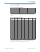
Table 7–1 describes the functionality of the four user push buttons that control the
power design example. The on-board 50-MHz oscillator provides the input clock
(
i_clk
,
PIN_AH15
).
Table 7–1. Four Input Button Functionality
User Push
Button
FPGA Pin Type Description
User_PB0 AD7 Reset Resets the demo to the beginning,
i_nrst
User_PB1 AC12 Toggle
Advances the design example to the next higher frequency,
i_nfreq_next
User_PB2 AH3 Toggle
Advances the design example to the next higher resource utilization,
i_nperc_next
User_PB3 AA12 Toggle Enables the outputs to toggle,
i_noutput_ena