
User guide

6–8 Chapter 6: Board Test System
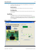
Using the Board Test System
Cyclone III FPGA Development Kit User Guide September 2010 Altera Corporation
To update the SRAM contents, change values in the table and click Write. The
application writes the new values to SRAM and then reads the values back to
guarantee that the graphical display accurately reflects the memory contents.
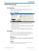
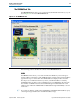
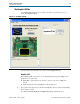
Flash
The Flash control allows you to read and write the flash memory on your board. Type
a starting address in the text box and click Read. Values starting at the specified
address appear in the top row of the table. The flash memory addresses display in the
format the Nios II processor within the FPGA uses, that is, each flash memory address
is offset by 0x00000000. Thus, the first location in flash memory appears as 0x00000000
in the GUI. The base address of flash memory in this Nios II-based BTS design is
0x0800.0000. The valid address range within the 64-MB flash memory is 0x0000.0000
through 0x03FF.FFFF, as shown in the GUI.
1 If you enter an address outside of the 0x00000000 to 0x03FFFF80 flash memory
address space, a warning message identifies the valid flash memory address range.
To update the flash memory contents, change values in the table and click Write. The
application writes the new values to flash memory and then reads the values back to
guarantee that the graphical display accurately reflects the memory contents.
1 To prevent overwriting the dedicated portions of flash memory, the application limits
the writable flash memory address range from 0x07000000 to 0x0701FF80 (which
corresponds to the unused flash memory address range of 0x02000000 - 0x0201FF80
shown in Figure 6–1 on page 6–2).