
User guide

Chapter 6: Board Test System 6–5
Using the Board Test System
September 2010 Altera Corporation Cyclone III FPGA Development Kit User Guide
1 Connecting a jumper shunt on J6 and an external USB-Blaster on J14 includes the
MAX II device in the JTAG chain.
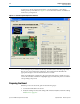
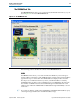
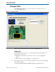
Board Information
The Board information controls display static information about your board.
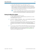
Flash Memory Map
The Flash memory map control shows the memory map of the flash memory device
on your board.
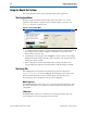
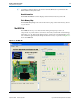
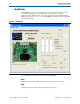
The GPIO Tab
The GPIO tab allows you to interact with all the general purpose user I/O
components on your board. You can write to the LCD, read user DIP switch settings,
turn LEDs on or off, detect push button presses, write to the 7-segment display, and
run an Ethernet application (the Simple Socket Server Test) on your board. Figure 6–3
shows the GPIO tab.
Figure 6–3. The GPIO Tab