
User guide


5–2 Chapter 5: Board Update Portal
Using the Board Update Portal to Update User Designs
Cyclone III FPGA Development Kit User Guide September 2010 Altera Corporation
5. Click Cyclone III FPGA Development Kit on the Board Update Portal web page
to access the kit’s home page. Visit this page occasionally for documentation
updates and additional new designs.
f You can also navigate directly to the Cyclone III FPGA Development Kit page of the
Altera website to determine if you have the latest kit software.
Using the Board Update Portal to Update User Designs
The Board Update Portal allows you to write new designs to the FPGA design 1 and
design 6 (HW1 and SW1)portion of flash memory. Designs must be in the Nios II
Flash Programmer File (.flash) format.
1 Design files available from the Cyclone III FPGA Development Kit page of the Altera
website include .flash files. You can also create .flash files from your own custom
design. Refer to “Creating a Flash File” on page A–1 for information about preparing
your own design for upload.
To upload a design over the network into the FPGA design 1 and design 6 (HW1 and
SW1) of flash memory on your board, perform the following steps:
1. Perform the steps in “Connecting to the Board Update Portal Web Page” to access
the Board Update Portal web page.
2. In the Hardware File Name field specify the .flash file that you either downloaded
from the Altera website or created on your own. If there is a software component
to the design, specify it in the same manner using the Software File Name field,
otherwise leave the Software File Name field blank.
3. Click Upload. The file takes about 20 seconds to upload.
4. To configure the FPGA with the new design after the flash memory upload process
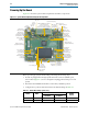
completes, set the PGM CONFIG SELECT rotary switch (SW5) to the 1 position
and power cycle the board, or press the RESET_CONFIG push-button (S6).
1 As long as you do not overwrite the factory image in the flash memory device, you
can continue to use the Board Update Portal to write new designs to the FPGA
design 1 and design 6 (HW1 and SW1)portion of flash memory. If you overwrite the
factory image, you can restore it by following the instructions in “Restoring the
Factory Design to the Flash Device” on page A–6.