
User guide

Chapter 4: Development Board Setup 4–3
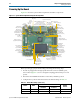
Powering Up the Board
September 2010 Altera Corporation Cyclone III FPGA Development Kit User Guide
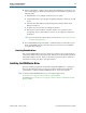
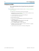
4. Ensure that the 4-position SW3 mini-DIP switches and the two jumpers are set to
the default positions shown in Table 4–2.
5. Verify that the PGM CONFIG SELECT rotary switch SW5 is set to 0.
At power up, the development board uses a preloaded configuration to demonstrate
that the board is operating correctly.
Power up the development board by performing the following steps:
1. Connect the 16-V DC adapter to the development board and to a power source.
w Use only the supplied 16-V power supply. Power regulation circuitry on the board
could be damaged by supplies greater than 16 V.
2. Slide the POWER switch to ON. The nearby blue POWER light-emitting diode
(LED) lights up.
3. Confirm that user LEDs 0-7 flash in a scrolling, side-to-side pattern. For
customized configurations, the pattern depends on the application.
f For information about custom configurations, refer to “Programming the
Flash Device” on page A–4.
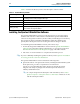
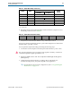
3RSV0
MAX_RESERVE0
X
4RSV1
MAX_RESERVE1
X
5 MAX0 PFL Disable PFL Enable 1
6 MAX1
MAX_DIP1
X
7 MAX2
MAX_DIP2
X
8 MAX3
MAX_DIP3
X
Note to Table 4–1:
(1) X = don’t care
Table 4–2. Initial Switch and Jumper Settings
DEV_SEL-J6 JTAG_SEL-J7 SW3.1 SW3.2 SW3.3 SW3.4
ON ON ON OFF OFF OFF
Table 4–1. Switch SW1 Settings (Part 2 of 2)
Switch Name
Function
Default
Position
Position 0 Position 1