
User guide

4–2 Chapter 4: Development Board Setup
Powering Up the Board
Cyclone III FPGA Development Kit User Guide September 2010 Altera Corporation
Powering Up the Board
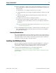
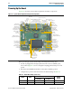
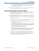
Figure 4–1 shows the Cyclone III development board and its components.
Before powering up, prepare the board by performing the following steps:
1. If cards are plugged into the high-speed mezzanine connector (HSMC) ports,
remove them (Figure 4–1) shows a daughter card plugged into both port A and
port B).
2. Ensure that the POWER switch SW2 is in the OFF (or DOWN) position.
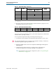
3. Configure the 8-position SW1 DIP switch to the default settings in Table 4–1.
Figure 4–1. Cyclone III Development Board Layout and Components
Speaker Header (J5)
DC Power
Jack (J2)
Ethernet PHY
LEDs (D1, D3, D4)
Ethernet PHY
Duplex LED (D6)
Power
Switch (SW2)
Power
LED (D5)
Ethernet PHY TX/RX
Activity LEDS (D7, D8)
MAX II CPLD (U7)
DDR2 SDRAM Device Interface
Four x16 and one x8
(U11, U12, U25, U26, U13)
(Three on Top and Two on Bottom)
DDR2TOP_ACTIVE
LED (D11)
Cyclone III FPGA (U20)
MAX II Device
Control DIP
Switch (SW1)
24-MHz Crystal (Y1)
6-MHz
Crystal (Y2)
Clock Out SMA (J11)
HSMC Port B
Present LED (D19)
PGM Config Select
Rotary Switch (SW5)
User Push Buttons
(S1 through S4)
User DIP
Switch (SW6)
CPU Reset Push
Button Switch (S5)
Power Select
Rotary Switch (SW4)
User Defined
7-Segment
Display (U30)
Board-Specific LEDs
(D20 through D24)
SRAM Active
LED (D17)
HSMC Port A
Present LED (D18)
Clock In SMA (J10)
Power Display (U28)
Flash Active
LED (D23)
Configuration
Done LED (D25)
User LEDs
(D26 through D33)
Reset and
Factory
Configuration
Push Buttons
(S6 and S7)
DDR2BOT_ACTIVE
LED (D16)
50-MHz
Clock (Y5)
125-MHz
Clock (Y4)
24-MHz USB-
Blaster Clock (Y3)
JTAG Control
DIP Switch (SW3)
Graphics
LCD (J13)
HSMC Port B (J9)
(Debug Header Shown)
HSMC Port A (J8)
(Loopback Board Shown)
Device Select
Jumper (J6)
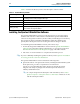
Table 4–1. Switch SW1 Settings (Part 1 of 2)
Switch Name
Function
Default
Position
Position 0 Position 1
1mΩ/mA mΩ mA 0
2V/Ω VW1