
User guide


4–2 Altera Corporation
Cyclone III FPGA Starter Kit User Guide July 2010
Measuring Power
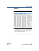
The design used for power measurement is a replicated set of randomly
filled ROMs that feed a multiplier block and a shift register that is fed by
a signal that changes every clock cycle. Tables 4–2 and 4–3 show the
power state which represent the percent of the full design used. As
compiled, this full design uses:
■ Logic elements: 22,493/24,624 (91%)
■ Combinational functions: 1,961/24,624 (8%)
■ Dedicated logic registers: 21,133/24,624 (86%)
■ Total registers: 21,133
■ Total pins: 73/216 (34%)
■ Total memory bits: 524,288/608,256 (86%)
■ Embedded Multiplier 9-bit elements: 128/132 (97 %)
■ Total PLLs: 1/4 (25%)
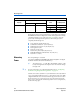
Measuring
Power
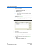
The example design is located in
<kit install>\examples\cycloneIII_3c25_start_power_demo. Configure
the FPGA with the .sof found in the directory.
1 The input clock (i_clk PIN_B9) is the 50-MHz oscillator on the
board, which generates the input clock for the reference design
through a PLL
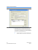
f For more information on configuring the FPGA, refer to “Configuring
the FPGA Using the Quartus II Programmer” on page 2–3.
Current sense resistors (0.010 ± 1%) are installed at locations JP6 (FPGA
core power) and JP3 (FPGA I/O power + other device I/O power). With
a digital multimeter set to mV measurement range, the resistor at location
JP6 measures the core power. The resistor at location JP3 measures the
I/O power. To measure the current being used in various configurations,
use the following steps:
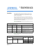
Table 4–3. LEDs Power State (Resources)
Displays
LEDs
State % of Design Used
MSB LSB
Resources LED4 LED3 00 25%
01 50%
10 75%
11 100%