Cyclone III FPGA Starter Kit User Guide 101 Innovation Drive San Jose, CA 95134 www.altera.com P25-36228-03 Document Version: Document Date: 1.
© 2010 Altera Corporation. All rights reserved. ALTERA, ARRIA, CYCLONE, HARDCOPY, MAX, MEGACORE, NIOS, QUARTUS and STRATIX are Reg. U.S. Pat. & Tm. Off. and/or trademarks of Altera Corporation in the U.S. and other countries. All other trademarks and service marks are the property of their respective holders as described at www.altera.com/common/legal.html.
Contents Chapter 1. Getting Started Introduction ............................................................................................................................................ 1–1 Before You Begin ................................................................................................................................... 1–2 Further Information ..............................................................................................................................
Contents Chapter 4. Measuring Power on the Cyclone III Starter Board Introduction ............................................................................................................................................ 4–1 Measuring Power ................................................................................................................................... 4–2 Changing the Example Design .......................................................................................................
1. Getting Started Introduction Welcome to the Altera® Cyclone® III FPGA Starter Kit, which includes a full-featured field-programmable gate array (FPGA) development board, hardware and software development tools, documentation, and accessories needed to begin FPGA development. The development board includes an Altera Cyclone III FPGA and comes preconfigured with a hardware reference design stored in flash memory. You can use the development board as a platform to prototype a variety of FPGA designs.
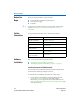
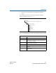
Before You Begin Before You Begin Before proceeding, check the contents of the kit: ■ ■ ■ f Further Information Cyclone III FPGA Starter Development Board 12-V DC power supply USB cable For the most up-to-date information on this product, visit the Altera website at www.altera.com/products/devkits/altera/kit-cyc3starter.html. For other related information, refer to the following websites: For More Information About Refer To Additional daughter cards available for purchase www.altera.
Getting Started 2. Follow the on-screen instructions to complete the installation process. The installation program creates the Cyclone III FPGA Starter Kit directory structure shown in Figure 1–1. Figure 1–1. Cyclone III FPGA Starter Kit Default Installed Directory Structure The default Windows installation directory is C:\altera\\.
Software Installation Installing the Quartus II Web Edition Software The Quartus II Web Edition software provides the necessary tools for developing hardware and software for Altera FPGAs. Included in the Quartus II Web Edition software are the Quartus II software, the Nios II EDS, and the MegaCore® IP Library. The Quartus II software (including SOPC Builder) and the Nios II EDS are the primary FPGA development tools for creating the reference designs in this kit.
Getting Started ■ 1 The OpenCore Plus hardware evaluation feature is an evaluation tool for prototyping only. You must purchase a license to use a MegaCore function in production. f For more information about OpenCore Plus, refer to AN 320: OpenCore Plus Evaluation of Megafunctions. Nios® II Embedded Design Suite (EDS)—A full-featured tool set that allows you to develop embedded software for the Nios II processor which you can include in your Altera FPGA designs.
Software Installation 1–6 Cyclone III FPGA Starter Kit User Guide Altera Corporation July 2010
2. Development Board and Control Panel Setup Development Board Setup The development board is preloaded with an example design to demonstrate the Cyclone® III device and board features. At power-up, the preloaded design also enables you to quickly confirm that the board is operating correctly. Figure 2–1 shows the Cyclone III development board layout and components. Figure 2–1.
Installing the USB-Blaster Driver Requirements Before you proceed, ensure that the follwing items are installed: ■ ■ ■ Altera® Quartus® II software on the host computer Cyclone III FPGA Starter Kit USB-Blaster™ driver software on the host computer. The Cyclone III FPGA starter development board includes an integrated USB-Blaster circuitry for FPGA programming. Powering Up the Development Board To power-up the development board, follow these steps: 1.
Development Board and Control Panel Setup Control Panel Setup Setting up the control panel involves the following: ■ ■ 1 Configuring the FPGA Starting the control panel Power up the board and ensure that is is operational. For more information about using the control panel, refer to the “Using the Control Panel” chapter. Configuring the FPGA Using the Quartus II Programmer You can use the Quartus II Programmer to configure the FPGA with a specific .sof.
Configuring the FPGA Using the Quartus II Programmer 2–4 Cyclone III FPGA Starter Kit User Guide Altera Corporation July 2010
3. Using the Control Panel Overview The control panel consists of the following: ■ ■ The graphical user interface (GUI) application on the host computer The standard Nios II hardware design running on the board's Cyclone III FPGA device After installing the Cyclone III FPGA Starter Kit, you can locate the control panel for the hardware and software in the \demos\control_panel directory.
LEDs and Buttons You can locate the source for the example design in the \examples\cycloneIII_3c25_starter_board_standard directory. 1 To launch the control panel user interface, run the control_panel.exe program found in the \demos\control_panel directory (Figure 3–1). Figure 3–1. Control Panel Window LEDs and Buttons Illuminating LEDs To illuminate an LED, follow these steps: 1. The LED & Buttons tab should be visible when the application runs.
Using the Control Panel Buttons Indicators 1. Press the push-button switches on the board. Notice that buttons on the GUI change accordingly. Figure 3–2.
DDR SDRAM/ SSRAM/On-Chip Controller The following sections describe how to access the DDR SDRAM. You can use the same procedure to access the SSRAM. Read/Write Data To read from and write to the DDR SDRAM, follow these steps: 1. Click the DDR SDRAM tab (Figure 3–3). The Address column indicates the hex address of the DDR SDRAM. The values inside the 0-3, 4-7, 8-B, and C-F columns are the DDR SDRAM contents in hex words format. Figure 3–3. Control Panel DDR SDRAM Tab 2.
Using the Control Panel Read from a File To read the contents of a file and load it to the DDR SDRAM, follow these steps: 1. Click Load File. 2. Browse to sample.txt located in the control_panel directory and click Open. This step instantiates the DDR SDRAM controller and loads the text contents into the DDR SDRAM. Notice that the Data to Ascii-text column shows the DDR SDRAM contents in Ascii value.
Flash Memory Programmer Flash Memory Tab To use the flash memory functions, click the Flash Memory tab (Figure 3–4). Figure 3–4. Control Panel Flash Memory Tab CFI Query The common flash interface (CFI) flash memory devices conform to basic flash commands. The most basic command is Query which switches the device into a ROM table mode so that features of the flash device are determined by reading values from the table. To perform a CFI query using the host application, click CFI Query.
Using the Control Panel Read/Write Data To read from and write to the flash memory, follow these steps: Figure 3–5. Control Panel Flash Memory Tab Altera Corporation July 2010 1. Click Erase Block to perform a block erase of the flash memory. The Address column indicates the hex address of the flash memory. The values inside the 0-3, 4-7, 8-B, and C-F columns are the flash memory contents in hex words format. 2.
Flash Memory Programmer 3–8 Cyclone III FPGA Starter Kit User Guide Altera Corporation July 2010
4. Measuring Power on the Cyclone III Starter Board Introduction One of the main features of the Cyclone® III device is its low power consumption. You can measure the power of the 3C25 device on the Cyclone III starter board under various conditions with an example design provided with the kit. The power example design allows you to control the amount of logic utilized in the FPGA, the clock frequency, the number of I/Os being used, and measure the effect on the power to the Cyclone III device.
Measuring Power Table 4–3. LEDs Power State (Resources) LEDs Displays Resources MSB LSB LED4 LED3 State % of Design Used 00 25% 01 50% 10 75% 11 100% The design used for power measurement is a replicated set of randomly filled ROMs that feed a multiplier block and a shift register that is fed by a signal that changes every clock cycle. Tables 4–2 and 4–3 show the power state which represent the percent of the full design used.
Measuring Power on the Cyclone III Starter Board 1 To obtain the power (P) in milliwatts, measure (the voltage across the sense resistors at JP6 or JP3) in mV and calculate the nominal power using the equation: P = 100 x x where is 1.2 V for JP6 and 2.5 V for JP3. You can use the four input buttons to advance through the various power state as outlined in Table 4–2.
Measuring Power 4–4 Cyclone III FPGA Starter Kit User Guide Altera Corporation July 2010
Appendix A. Programming the Configuration Flash Device Overview The Intel® P30 flash device uses active parallel flash configuration to configure the Cyclone® III device on power up. The Cyclone III Starter Board has a factory default configuration programmed into the P30 flash; however, after developing your own project, you may want to replace this factory default configuration with your own. This appendix describes how to reprogram the Intel P30 flash device.
Creating a Flash-Programmable POF File 2. Select the following settings: ● ● ● ● Programming File Type: Programmer Object File (.pof) Configuration Device: CFI_128MB Mode: Active Parallel File Name: Type the name of the flashable .pof to write 1 3. If you choose to overwrite the existing .pof, a warning message occurs. Under Input file to the convert, select Configuration Master under SOF Data. Refer to Figure A–2.
Figure A–3. SOF Data Properties 1 8. Altera Corporation July 2010 The flash address 0x20000 is the default starting address from which the Cyclone III device starts loading configuration data. Click OK. Figure A–4 shows the updated Convert Programming Files window.
Creating a Flash-Programmable POF File Figure A–4. Updated Convert Programming Files Window 9. Click Generate. If you are overwriting the input .pof you will receive a warning asking if you want to overwrite it. Click Yes to overwrite the file or enter a different filename. When the Quartus II software finishes converting the file, you can use the converted .pof to program the on-board parallel flash device.
Programming the Flash Device Altera recommends that you do not overwrite the factory hardware and factory software images unless you are an expert with the Altera tools or deliberately overwriting the factory design. If you unintentionally overwrite the factory image, perform these flash programming instructions using the cycloneIII_3c25_start_niosII_standard.pof found in the factory_recovery directory for the object file in step 9. To program the flash device, follow these steps: 1.
Programming the Flash Device 7. In the Quartus II Programmer, select the CFI_128MB device. 8. Click Change File from the button list at the left of the programming file area. 9. Select the converted .pof that you generated in the previous section. 1 To restore factory flash contents, choose cycloneIII_3c25_start_niosII_standard.pof located in the factory_recovery directory as your converted .pof. 10. Turn on the Program/Configure option for all devices shown in the Programmer.
Additional Information Revision History The table below displays the revision history for the chapters in this user guide. Chapter Date Version All July 2010 1.2.0 Changes Made ● ● ● ● ● ● All March 2010 1.1.0 ● ● ● ● ● 1, 2, 4 June 2008 1.0.1 ● ● First publication. ● ● April 2007 Altera Corporation 1.0.0 Updated the directory structure in Figure 1–1. Updated “Control Panel Start” section and Figure 3–1. Updated “LEDs” section and Figure 3–2.
How to Contact Altera How to Contact Altera Cyclone III FPGA Starter Kit User Guide For the most up-to-date information about Altera products, refer to the following table. Contact Note (1) Contact Method Address Technical support Website www.altera.com/support Technical training Website www.altera.com/training Email custrain@altera.com Product literature Website www.altera.com/literature Non-technical support (General) Email nacomp@altera.
Additional Information Visual Cue Courier type Typographic Conventions Meaning Signal and port names are shown in lowercase Courier type. Examples: data1, tdi, input. Active-low signals are denoted by suffix n, e.g., resetn. Anything that must be typed exactly as it appears is shown in Courier type. For example: c:\qdesigns\tutorial\chiptrip.gdf. Also, sections of an actual file, such as a Report File, references to parts of files (e.g., the AHDL keyword SUBDESIGN), as well as logic function names (e.g.
Typographic Conventions Info–iv Preliminary Cyclone III FPGA Starter Kit User Guide Altera Corporation