
Datasheet
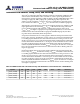

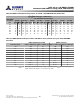
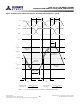
Table Of Contents
- DDR3L SDRAM
- Description
- State Diagram
- Functional Description
- Functional Block Diagrams
- Ball Assignments and Descriptions
- Package Dimensions
- Electrical Specifications
- Thermal Characteristics
- Electrical Specifications – I DD Specifications and Conditions
- Electrical Characteristics – 1.35V IDD Specifications
- Electrical Specifications – DC and AC
- ODT Characteristics
- Output Driver Impedance
- Output Characteristics and Operating Conditions
- Speed Bin Tables
- Electrical Characteristics and AC Operating Conditions
- Electrical Characteristics and AC Operating Conditions
- Command and Address Setup, Hold, and Derating
- Data Setup, Hold, and Derating
- Commands – Truth Tables
- Commands
- Input Clock Frequency Change
- Write Leveling
- Initialization
- Voltage Initialization / Change
- Mode Registers
- Mode Register 0 (MR0)
- Mode Register 1 (MR1)
- Mode Register 2 (MR2)
- Mode Register 3 (MR3)
- MODE REGISTER SET (MRS) Command
- ZQ CALIBRATION Operation
- ACTIVATE Operation
- READ Operation
- WRITE Operation
- PRECHARGE Operation
- SELF REFRESH Operation
- Extended Temperature Usage
- Power-Down Mode
- RESET Operation
- On-Die Termination (ODT)
- Dynamic ODT
- Synchronous ODT Mode
- Asynchronous ODT Mode
- Asynchronous to Synchronous ODT Mode Transition (Power-Down Exit)
Table 60: DDR3L-1866/2133 Derating Values for
t
IS/
t
IH – AC125/DC90-Based (Continued)
Δ
Δ
t
IS,
Δ
t
IH Derating (ps) – AC/DC-Based
CMD/ADDR
Slew Rate
V/ns
CK, CK# Differential Slew Rate
4.0 V/ns 3.0 V/ns 2.0 V/ns 1.8 V/ns 1.6 V/ns 1.4 V/ns 1.2 V/ns 1.0 V/ns
Δ
t
IS
Δ
t
IH
Δ
t
IS
Δ
t
IH
Δ
t
IS
Δ
t
IH
Δ
t
IS
Δ
t
IH
Δ
t
IS
Δ
t
IH
Δ
t
IS
Δ
t
IH
Δ
t
IS
Δ
t
IH
Δ
t
IS
Δ
t
IH
0.9 3 –3 3 –3 3 –311 5 1913272135314347
0.8 6 –8 6 –8 6 –8 14 1 22 9 30 17 38 27 46 43
0.7 10 –13 10 –13 10 –13 18 –5 26 3 34 11 42 21 50 37
0.6 16 –20 16 –20 16 –20 24 –12 32 –4 40 4 48 14 56 30
0.5 15 –30 15 –30 15 –30 23 –22 31 –14 39 –6 47 4 55 20
0.4 13 –45 13 –45 13 –45 21 –37 29 –29 37 –21 45 –11 53 5
Table 61: DDR3L Minimum Required Time
t
VAC Above V
IH(AC)
(Below V
IL[AC]
) for Valid ADD/CMD
Transition
Slew Rate (V/ns)
DDR3L-800/1066/1333/1600 DDR3L-1866/2133
t
VAC at 160mV (ps)
t
VAC at 135mV (ps)
t
VAC at 135mV (ps)
t
VAC at 125mV (ps)
>2.0 200 213 200 205
2.0 200 213 200 205
1.5 173 190 178 184
1.0 120 145 133 143
0.9 102 130 118 129
0.8 80 111 99 111
0.7 51 87 75 89
0.6 13 55 43 59
0.5 Note 1 10 Note 1 18
<0.5 Note 1 10 Note 1 18
Note:
1. Rising input signal shall become equal to or greater than V
IH(AC)
level and Falling input
signal shall become equal to or less than V
IL(AC)
level.
8Gb: x4, x8, x16 DDR3L SDRAM
Command and Address Setup, Hold, and Derating
95
Rev 2.0 June 2016
© 2015 Alliance Memory, Inc. All rights reserved.
Alliance Memory Inc. reserves the right to change products or specification without notice
Alliance Memory Inc. 511 Taylor Way, San Carlos, CA 94070
TEL: (650) 610-6800 FAX: (650) 620-9211