
Datasheet
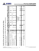
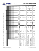

Table Of Contents
- DDR3L SDRAM
- Description
- State Diagram
- Functional Description
- Functional Block Diagrams
- Ball Assignments and Descriptions
- Package Dimensions
- Electrical Specifications
- Thermal Characteristics
- Electrical Specifications – I DD Specifications and Conditions
- Electrical Characteristics – 1.35V IDD Specifications
- Electrical Specifications – DC and AC
- ODT Characteristics
- Output Driver Impedance
- Output Characteristics and Operating Conditions
- Speed Bin Tables
- Electrical Characteristics and AC Operating Conditions
- Electrical Characteristics and AC Operating Conditions
- Command and Address Setup, Hold, and Derating
- Data Setup, Hold, and Derating
- Commands – Truth Tables
- Commands
- Input Clock Frequency Change
- Write Leveling
- Initialization
- Voltage Initialization / Change
- Mode Registers
- Mode Register 0 (MR0)
- Mode Register 1 (MR1)
- Mode Register 2 (MR2)
- Mode Register 3 (MR3)
- MODE REGISTER SET (MRS) Command
- ZQ CALIBRATION Operation
- ACTIVATE Operation
- READ Operation
- WRITE Operation
- PRECHARGE Operation
- SELF REFRESH Operation
- Extended Temperature Usage
- Power-Down Mode
- RESET Operation
- On-Die Termination (ODT)
- Dynamic ODT
- Synchronous ODT Mode
- Asynchronous ODT Mode
- Asynchronous to Synchronous ODT Mode Transition (Power-Down Exit)
Table 56: Electrical Characteristics and AC Operating Conditions for Speed Extensions (Continued)
Notes 1–8 apply to the entire table
Parameter Symbol
DDR3L-1866 DDR3L-2133
Unit NotesMin Max Min Max
ACTIVATE-to-ACTIVATE
minimum command pe-
riod
x4/x8/x16
(2KB page size)
t
RRD MIN = greater of 4CK or 6ns CK 31
Four ACTIVATE
windows
x4/x8/x16
(2KB page size)
t
FAW 35 – 35 – ns 31
Write recovery time
t
WR MIN = 15ns; MAX = N/A ns 31, 32,
33
Delay from start of internal WRITE transac-
tion to internal READ command
t
WTR MIN = greater of 4CK or 7.5ns; MAX = N/A CK 31, 34
READ-to-PRECHARGE time
t
RTP MIN = greater of 4CK or 7.5ns; MAX = N/A CK 31, 32
CAS#-to-CAS# command delay
t
CCD MIN = 4CK; MAX = N/A CK
Auto precharge write recovery + precharge
time
t
DAL MIN = WR +
t
RP/
t
CK (AVG); MAX = N/A CK
MODE REGISTER SET command cycle time
t
MRD MIN = 4CK; MAX = N/A CK
MODE REGISTER SET command update delay
t
MOD MIN = greater of 12CK or 15ns; MAX = N/A CK
MULTIPURPOSE REGISTER READ burst end to
mode register set for multipurpose register
exit
t
MPRR MIN = 1CK; MAX = N/A CK
Calibration Timing
ZQCL command: Long
calibration time
POWER-UP and RE-
SET operation
t
ZQinit MIN = N/A
MAX = MAX(512nCK, 640ns)
CK
Normal operation
t
ZQoper MIN = N/A
MAX = max(256nCK, 320ns)
CK
ZQCS command: Short calibration time MIN = N/A
MAX = max(64nCK, 80ns)
t
ZQCS
CK
Initialization and Reset Timing
Exit reset from CKE HIGH to a valid command
t
XPR MIN = greater of 5CK or
t
RFC + 10ns; MAX = N/A CK
Begin power supply ramp to power supplies
stable
t
VDDPR MIN = N/A; MAX = 200 ms
RESET# LOW to power supplies stable
t
RPS MIN = 0; MAX = 200 ms
RESET# LOW to I/O and R
TT
High-Z
t
IOZ MIN = N/A; MAX = 20 ns 35
Refresh Timing
8Gb: x4, x8, x16 DDR3L SDRAM
Electrical Characteristics and AC Operating Conditions
86
Rev 2.0 June 2016
© 2015 Alliance Memory, Inc. All rights reserved.
Alliance Memory Inc. reserves the right to change products or specification without notice
Alliance Memory Inc. 511 Taylor Way, San Carlos, CA 94070
TEL: (650) 610-6800 FAX: (650) 620-9211