
Datasheet
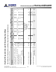
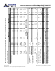
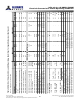

Table Of Contents
- DDR3L SDRAM
- Description
- State Diagram
- Functional Description
- Functional Block Diagrams
- Ball Assignments and Descriptions
- Package Dimensions
- Electrical Specifications
- Thermal Characteristics
- Electrical Specifications – I DD Specifications and Conditions
- Electrical Characteristics – 1.35V IDD Specifications
- Electrical Specifications – DC and AC
- ODT Characteristics
- Output Driver Impedance
- Output Characteristics and Operating Conditions
- Speed Bin Tables
- Electrical Characteristics and AC Operating Conditions
- Electrical Characteristics and AC Operating Conditions
- Command and Address Setup, Hold, and Derating
- Data Setup, Hold, and Derating
- Commands – Truth Tables
- Commands
- Input Clock Frequency Change
- Write Leveling
- Initialization
- Voltage Initialization / Change
- Mode Registers
- Mode Register 0 (MR0)
- Mode Register 1 (MR1)
- Mode Register 2 (MR2)
- Mode Register 3 (MR3)
- MODE REGISTER SET (MRS) Command
- ZQ CALIBRATION Operation
- ACTIVATE Operation
- READ Operation
- WRITE Operation
- PRECHARGE Operation
- SELF REFRESH Operation
- Extended Temperature Usage
- Power-Down Mode
- RESET Operation
- On-Die Termination (ODT)
- Dynamic ODT
- Synchronous ODT Mode
- Asynchronous ODT Mode
- Asynchronous to Synchronous ODT Mode Transition (Power-Down Exit)
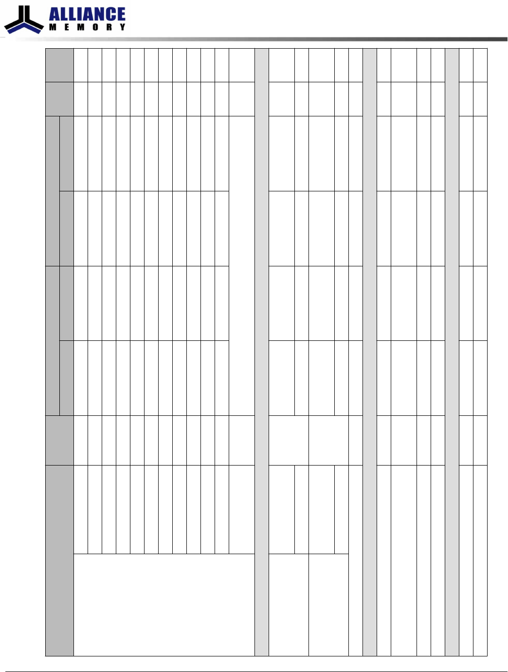
Table 56: Electrical Characteristics and AC Operating Conditions for Speed Extensions (Continued)
Notes 1–8 apply to the entire table
Parameter Symbol
DDR3L-1866 DDR3L-2133
Unit NotesMin Max Min Max
Cumulative error across 2 cycles
t
ERR2per –88 88 –74 74 ps 17
3 cycles
t
ERR3per –105 105 –87 87 ps 17
4 cycles
t
ERR4per –117 117 –97 97 ps 17
5 cycles
t
ERR5per –126 126 –105 105 ps 17
6 cycles
t
ERR6per –133 133 –111 111 ps 17
7 cycles
t
ERR7per –139 139 –116 116 ps 17
8 cycles
t
ERR8per –145 145 –121 121 ps 17
9 cycles
t
ERR9per –150 150 –125 125 ps 17
10 cycles
t
ERR10per –154 154 –128 128 ps 17
11 cycles
t
ERR11per –158 158 –132 132 ps 17
12 cycles
t
ERR12per –161 161 –134 134 ps 17
n = 13, 14 . . . 49, 50
cycles
t
ERRnper
t
ERRnper MIN = (1 + 0.68ln[n]) ×
t
JITper MIN
t
ERRnper MAX = (1 + 0.68ln[n]) ×
t
JITper MAX
ps 17
DQ Input Timing
Data setup time to
DQS, DQS#
Base (specification)
@ 2 V/ns
t
DS
(AC130)
70 – 55 – ps 18, 19
V
REF
@ 2 V/ns 135 – 120.5 – ps 19, 20
Data hold time from
DQS, DQS#
Base (specification)
@ 2 V/ns
t
DH
(DC90)
75 – 60 – ps 18, 19
V
REF
@ 2 V/ns 110 – 105 – ps 19, 20
Minimum data pulse width
t
DIPW 320 – 280 – ps 41
DQ Output Timing
DQS, DQS# to DQ skew, per access
t
DQSQ – 85 – 75 ps
DQ output hold time from DQS, DQS#
t
QH 0.38 – 0.38 –
t
CK
(AVG)
21
DQ Low-Z time from CK, CK#
t
LZDQ –390 195 –360 180 ps 22, 23
DQ High-Z time from CK, CK#
t
HZDQ – 195 – 180 ps 22, 23
DQ Strobe Input Timing
DQS, DQS# rising to CK, CK# rising
t
DQSS –0.27 0.27 –0.27 0.27 CK 25
DQS, DQS# differential input low pulse width
t
DQSL 0.45 0.55 0.45 0.55 CK
8Gb: x4, x8, x16 DDR3L SDRAM
Electrical Characteristics and AC Operating Conditions
84
Rev 2.0 June 2016
© 2015 Alliance Memory, Inc. All rights reserved.
Alliance Memory Inc. reserves the right to change products or specification without notice
Alliance Memory Inc. 511 Taylor Way, San Carlos, CA 94070
TEL: (650) 610-6800 FAX: (650) 620-9211