
Datasheet
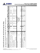
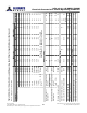
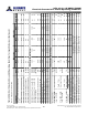
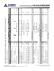
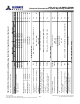

Table Of Contents
- DDR3L SDRAM
- Description
- State Diagram
- Functional Description
- Functional Block Diagrams
- Ball Assignments and Descriptions
- Package Dimensions
- Electrical Specifications
- Thermal Characteristics
- Electrical Specifications – I DD Specifications and Conditions
- Electrical Characteristics – 1.35V IDD Specifications
- Electrical Specifications – DC and AC
- ODT Characteristics
- Output Driver Impedance
- Output Characteristics and Operating Conditions
- Speed Bin Tables
- Electrical Characteristics and AC Operating Conditions
- Electrical Characteristics and AC Operating Conditions
- Command and Address Setup, Hold, and Derating
- Data Setup, Hold, and Derating
- Commands – Truth Tables
- Commands
- Input Clock Frequency Change
- Write Leveling
- Initialization
- Voltage Initialization / Change
- Mode Registers
- Mode Register 0 (MR0)
- Mode Register 1 (MR1)
- Mode Register 2 (MR2)
- Mode Register 3 (MR3)
- MODE REGISTER SET (MRS) Command
- ZQ CALIBRATION Operation
- ACTIVATE Operation
- READ Operation
- WRITE Operation
- PRECHARGE Operation
- SELF REFRESH Operation
- Extended Temperature Usage
- Power-Down Mode
- RESET Operation
- On-Die Termination (ODT)
- Dynamic ODT
- Synchronous ODT Mode
- Asynchronous ODT Mode
- Asynchronous to Synchronous ODT Mode Transition (Power-Down Exit)

19. These parameters are measured from a data signal (DM, DQ0, DQ1, and so forth) transi-
tion edge to its respective data strobe signal (DQS, DQS#) crossing.
20. The setup and hold times are listed converting the base specification values (to which
derating tables apply) to V
REF
when the slew rate is 1 V/ns. These values, with a slew rate
of 1 V/ns, are for reference only.
21. When the device is operated with input clock jitter, this parameter needs to be derated
by the actual
t
JITper (larger of
t
JITper (MIN) or
t
JITper (MAX) of the input clock (output
deratings are relative to the SDRAM input clock).
22. Single-ended signal parameter.
23. The DRAM output timing is aligned to the nominal or average clock. Most output pa-
rameters must be derated by the actual jitter error when input clock jitter is present,
even when within specification. This results in each parameter becoming larger. The fol-
lowing parameters are required to be derated by subtracting
t
ERR10per (MAX):
t
DQSCK
(MIN),
t
LZDQS (MIN),
t
LZDQ (MIN), and
t
AON (MIN). The following parameters are re-
quired to be derated by subtracting
t
ERR10per (MIN):
t
DQSCK (MAX),
t
HZ (MAX),
t
LZDQS
(MAX),
t
LZDQ MAX, and
t
AON (MAX). The parameter
t
RPRE (MIN) is derated by subtract-
ing
t
JITper (MAX), while
t
RPRE (MAX) is derated by subtracting
t
JITper (MIN).
24. The maximum preamble is bound by
t
LZDQS (MAX).
25. These parameters are measured from a data strobe signal (DQS, DQS#) crossing to its re-
spective clock signal (CK, CK#) crossing. The specification values are not affected by the
amount of clock jitter applied, as these are relative to the clock signal crossing. These
parameters should be met whether clock jitter is present.
26. The
t
DQSCK (DLL_DIS) parameter begins CL + AL - 1 cycles after the READ command.
27. The maximum postamble is bound by
t
HZDQS (MAX).
28. Commands requiring a locked DLL are: READ (and RDAP) and synchronous ODT com-
mands. In addition, after any change of latency
t
XPDLL, timing must be met.
29.
t
IS (base) and
t
IH (base) values are for a single-ended 1 V/ns control/command/address
slew rate and 2 V/ns CK, CK# differential slew rate.
30. These parameters are measured from a command/address signal transition edge to its
respective clock (CK, CK#) signal crossing. The specification values are not affected by
the amount of clock jitter applied as the setup and hold times are relative to the clock
signal crossing that latches the command/address. These parameters should be met
whether clock jitter is present.
31. For these parameters, the DDR3L SDRAM device supports
t
nPARAM (nCK) = RU(
t
PARAM
[ns]/
t
CK[AVG] [ns]), assuming all input clock jitter specifications are satisfied. For exam-
ple, the device will support
t
nRP (nCK) = RU(
t
RP/
t
CK[AVG]) if all input clock jitter specifi-
cations are met. This means that for DDR3-800 6-6-6, of which
t
RP = 5ns, the device will
support
t
nRP = RU(
t
RP/
t
CK[AVG]) = 6 as long as the input clock jitter specifications are
met. That is, the PRECHARGE command at T0 and the ACTIVATE command at T0 + 6 are
valid even if six clocks are less than 15ns due to input clock jitter.
32. During READs and WRITEs with auto precharge, the DDR3 SDRAM will hold off the in-
ternal PRECHARGE command until
t
RAS (MIN) has been satisfied.
33. When operating in DLL disable mode, the greater of 4CK or 15ns is satisfied for
t
WR.
34. The start of the write recovery time is defined as follows:
• For BL8 (fixed by MRS or OTF): Rising clock edge four clock cycles after WL
• For BC4 (OTF): Rising clock edge four clock cycles after WL
• For BC4 (fixed by MRS): Rising clock edge two clock cycles after WL
35. RESET# should be LOW as soon as power starts to ramp to ensure the outputs are in
High-Z. Until RESET# is LOW, the outputs are at risk of driving and could result in exces-
sive current, depending on bus activity.
36. The refresh period is 64ms when T
C
is less than or equal to 85°C. This equates to an aver-
age refresh rate of 7.8125μs. However, nine REFRESH commands should be asserted at
least once every 70.3μs. When T
C
is greater than 85°C, the refresh period is 32ms.
8Gb: x4, x8, x16 DDR3L SDRAM
Electrical Characteristics and AC Operating Conditions
81
Rev 2.0 June 2016
© 2015 Alliance Memory, Inc. All rights reserved.
Alliance Memory Inc. reserves the right to change products or specification without notice
Alliance Memory Inc. 511 Taylor Way, San Carlos, CA 94070
TEL: (650) 610-6800 FAX: (650) 620-9211