
Datasheet
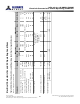
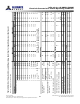
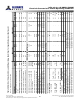
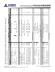
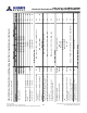

Table Of Contents
- DDR3L SDRAM
- Description
- State Diagram
- Functional Description
- Functional Block Diagrams
- Ball Assignments and Descriptions
- Package Dimensions
- Electrical Specifications
- Thermal Characteristics
- Electrical Specifications – I DD Specifications and Conditions
- Electrical Characteristics – 1.35V IDD Specifications
- Electrical Specifications – DC and AC
- ODT Characteristics
- Output Driver Impedance
- Output Characteristics and Operating Conditions
- Speed Bin Tables
- Electrical Characteristics and AC Operating Conditions
- Electrical Characteristics and AC Operating Conditions
- Command and Address Setup, Hold, and Derating
- Data Setup, Hold, and Derating
- Commands – Truth Tables
- Commands
- Input Clock Frequency Change
- Write Leveling
- Initialization
- Voltage Initialization / Change
- Mode Registers
- Mode Register 0 (MR0)
- Mode Register 1 (MR1)
- Mode Register 2 (MR2)
- Mode Register 3 (MR3)
- MODE REGISTER SET (MRS) Command
- ZQ CALIBRATION Operation
- ACTIVATE Operation
- READ Operation
- WRITE Operation
- PRECHARGE Operation
- SELF REFRESH Operation
- Extended Temperature Usage
- Power-Down Mode
- RESET Operation
- On-Die Termination (ODT)
- Dynamic ODT
- Synchronous ODT Mode
- Asynchronous ODT Mode
- Asynchronous to Synchronous ODT Mode Transition (Power-Down Exit)

Notes:
1. AC timing parameters are valid from specified T
C
MIN to T
C
MAX values.
2. All voltages are referenced to V
SS
.
3. Output timings are only valid for R
ON34
output buffer selection.
4. The unit
t
CK (AVG) represents the actual
t
CK (AVG) of the input clock under operation.
The unit CK represents one clock cycle of the input clock, counting the actual clock
edges.
5. AC timing and I
DD
tests may use a V
IL
-to-V
IH
swing of up to 900mV in the test environ-
ment, but input timing is still referenced to V
REF
(except
t
IS,
t
IH,
t
DS, and
t
DH use the
AC/DC trip points and CK, CK# and DQS, DQS# use their crossing points). The minimum
slew rate for the input signals used to test the device is 1 V/ns for single-ended inputs
and 2 V/ns for differential inputs in the range between V
IL(AC)
and V
IH(AC)
.
6. All timings that use time-based values (ns, μs, ms) should use
t
CK (AVG) to determine the
correct number of clocks (Table 55 (page 73) uses CK or
t
CK [AVG] interchangeably). In
the case of noninteger results, all minimum limits are to be rounded up to the nearest
whole integer, and all maximum limits are to be rounded down to the nearest whole
integer.
7. Strobe or DQS
diff
refers to the DQS and DQS# differential crossing point when DQS is
the rising edge. Clock or CK refers to the CK and CK# differential crossing point when
CK is the rising edge.
8. This output load is used for all AC timing (except ODT reference timing) and slew rates.
The actual test load may be different. The output signal voltage reference point is
V
DDQ
/2 for single-ended signals and the crossing point for differential signals (see Fig-
ure 27 (page 65)).
9.
When operating in DLL disable mode, Alliance Memory does not warrant compliance
with normal mode timings or functionality.
10. The clock’s
t
CK (AVG) is the average clock over any 200 consecutive clocks and
t
CK (AVG)
MIN is the smallest clock rate allowed, with the exception of a deviation due to clock
jitter. Input clock jitter is allowed provided it does not exceed values specified and must
be of a random Gaussian distribution in nature.
11. Spread spectrum is not included in the jitter specification values. However, the input
clock can accommodate spread-spectrum at a sweep rate in the range of 20–60 kHz with
an additional 1% of
t
CK (AVG) as a long-term jitter component; however, the spread
spectrum may not use a clock rate below
t
CK (AVG) MIN.
12. The clock’s
t
CH (AVG) and
t
CL (AVG) are the average half clock period over any 200 con-
secutive clocks and is the smallest clock half period allowed, with the exception of a de-
viation due to clock jitter. Input clock jitter is allowed provided it does not exceed values
specified and must be of a random Gaussian distribution in nature.
13. The period jitter (
t
JITper) is the maximum deviation in the clock period from the average
or nominal clock. It is allowed in either the positive or negative direction.
14.
t
CH (ABS) is the absolute instantaneous clock high pulse width as measured from one
rising edge to the following falling edge.
15.
t
CL (ABS) is the absolute instantaneous clock low pulse width as measured from one fall-
ing edge to the following rising edge.
16. The cycle-to-cycle jitter
t
JITcc is the amount the clock period can deviate from one cycle
to the next. It is important to keep cycle-to-cycle jitter at a minimum during the DLL
locking time.
17. The cumulative jitter error
t
ERRnper, where n is the number of clocks between 2 and 50,
is the amount of clock time allowed to accumulate consecutively away from the average
clock over n number of clock cycles.
18.
t
DS (base) and
t
DH (base) values are for a single-ended 1 V/ns slew rate DQs and 2 V/ns
slew rate differential DQS, DQS#; when DQ single-ended slew rate is 2V/ns, the DQS dif-
ferential slew rate is 4V/ns.
8Gb: x4, x8, x16 DDR3L SDRAM
Electrical Characteristics and AC Operating Conditions
80
Rev 2.0 June 2016
© 2015 Alliance Memory, Inc. All rights reserved.
Alliance Memory Inc. reserves the right to change products or specification without notice
Alliance Memory Inc. 511 Taylor Way, San Carlos, CA 94070
TEL: (650) 610-6800 FAX: (650) 620-9211