
Datasheet
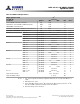
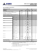

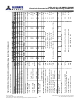
Table Of Contents
- DDR3L SDRAM
- Description
- State Diagram
- Functional Description
- Functional Block Diagrams
- Ball Assignments and Descriptions
- Package Dimensions
- Electrical Specifications
- Thermal Characteristics
- Electrical Specifications – I DD Specifications and Conditions
- Electrical Characteristics – 1.35V IDD Specifications
- Electrical Specifications – DC and AC
- ODT Characteristics
- Output Driver Impedance
- Output Characteristics and Operating Conditions
- Speed Bin Tables
- Electrical Characteristics and AC Operating Conditions
- Electrical Characteristics and AC Operating Conditions
- Command and Address Setup, Hold, and Derating
- Data Setup, Hold, and Derating
- Commands – Truth Tables
- Commands
- Input Clock Frequency Change
- Write Leveling
- Initialization
- Voltage Initialization / Change
- Mode Registers
- Mode Register 0 (MR0)
- Mode Register 1 (MR1)
- Mode Register 2 (MR2)
- Mode Register 3 (MR3)
- MODE REGISTER SET (MRS) Command
- ZQ CALIBRATION Operation
- ACTIVATE Operation
- READ Operation
- WRITE Operation
- PRECHARGE Operation
- SELF REFRESH Operation
- Extended Temperature Usage
- Power-Down Mode
- RESET Operation
- On-Die Termination (ODT)
- Dynamic ODT
- Synchronous ODT Mode
- Asynchronous ODT Mode
- Asynchronous to Synchronous ODT Mode Transition (Power-Down Exit)
Table 55: Electrical Characteristics and AC Operating Conditions (Continued)
Notes 1–8 apply to the entire table
Parameter Symbol
DDR3L-800 DDR3L-1066 DDR3L-1333 DDR3L-1600
Unit NotesMin Max Min Max Min Max Min Max
Exit self refresh to commands requiring a
locked DLL
t
XSDLL MIN =
t
DLLK (MIN); MAX = N/A CK 28
Minimum CKE low pulse width for self re-
fresh entry to self refresh exit timing
t
CKESR MIN =
t
CKE (MIN) + CK; MAX = N/A CK
Valid clocks after self refresh entry or power-
down entry
t
CKSRE MIN = greater of 5CK or 10ns; MAX = N/A CK
Valid clocks before self refresh exit,
power-down exit, or reset exit
t
CKSRX MIN = greater of 5CK or 10ns; MAX = N/A CK
Power-Down Timing
CKE MIN pulse width
t
CKE (MIN) Greater of 3CK
or 7.5ns
Greater of 3CK
or 5.625ns
Greater of 3CK
or 5.625ns
Greater of 3CK
or 5ns
CK
Command pass disable delay
t
CPDED MIN = 1; MAX = N/A CK
Power-down entry to power-down exit tim-
ing
t
PD MIN =
t
CKE (MIN); MAX = 9 * tREFI CK
Begin power-down period prior to CKE
registered HIGH
t
ANPD WL - 1CK CK
Power-down entry period: ODT either
synchronous or asynchronous
PDE Greater of
t
ANPD or
t
RFC - REFRESH command to CKE LOW time CK
Power-down exit period: ODT either
synchronous or asynchronous
PDX
t
ANPD +
t
XPDLL CK
Power-Down Entry Minimum Timing
ACTIVATE command to power-down entry
t
ACTPDEN MIN = 1 CK
PRECHARGE/PRECHARGE ALL command to
power-down entry
t
PRPDEN MIN = 1 CK
REFRESH command to power-down entry
t
REFPDEN MIN = 1 CK 37
MRS command to power-down entry
t
MRSPDEN MIN =
t
MOD (MIN) CK
READ/READ with auto precharge command
to power-down entry
t
RDPDEN MIN = RL + 4 + 1 CK
WRITE command to
power-down entry
BL8 (OTF, MRS)
BC4OTF
t
WRPDEN MIN = WL + 4 +
t
WR/
t
CK (AVG) CK
BC4MRS
t
WRPDEN MIN = WL + 2 +
t
WR/
t
CK (AVG) CK
8Gb: x4, x8, x16 DDR3L SDRAM
Electrical Characteristics and AC Operating Conditions
77
Rev 2.0 June 2016
© 2015 Alliance Memory, Inc. All rights reserved.
Alliance Memory Inc. reserves the right to change products or specification without notice
Alliance Memory Inc. 511 Taylor Way, San Carlos, CA 94070
TEL: (650) 610-6800 FAX: (650) 620-9211