
Datasheet
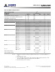
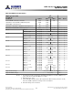

Table Of Contents
- DDR3L SDRAM
- Description
- State Diagram
- Functional Description
- Functional Block Diagrams
- Ball Assignments and Descriptions
- Package Dimensions
- Electrical Specifications
- Thermal Characteristics
- Electrical Specifications – I DD Specifications and Conditions
- Electrical Characteristics – 1.35V IDD Specifications
- Electrical Specifications – DC and AC
- ODT Characteristics
- Output Driver Impedance
- Output Characteristics and Operating Conditions
- Speed Bin Tables
- Electrical Characteristics and AC Operating Conditions
- Electrical Characteristics and AC Operating Conditions
- Command and Address Setup, Hold, and Derating
- Data Setup, Hold, and Derating
- Commands – Truth Tables
- Commands
- Input Clock Frequency Change
- Write Leveling
- Initialization
- Voltage Initialization / Change
- Mode Registers
- Mode Register 0 (MR0)
- Mode Register 1 (MR1)
- Mode Register 2 (MR2)
- Mode Register 3 (MR3)
- MODE REGISTER SET (MRS) Command
- ZQ CALIBRATION Operation
- ACTIVATE Operation
- READ Operation
- WRITE Operation
- PRECHARGE Operation
- SELF REFRESH Operation
- Extended Temperature Usage
- Power-Down Mode
- RESET Operation
- On-Die Termination (ODT)
- Dynamic ODT
- Synchronous ODT Mode
- Asynchronous ODT Mode
- Asynchronous to Synchronous ODT Mode Transition (Power-Down Exit)
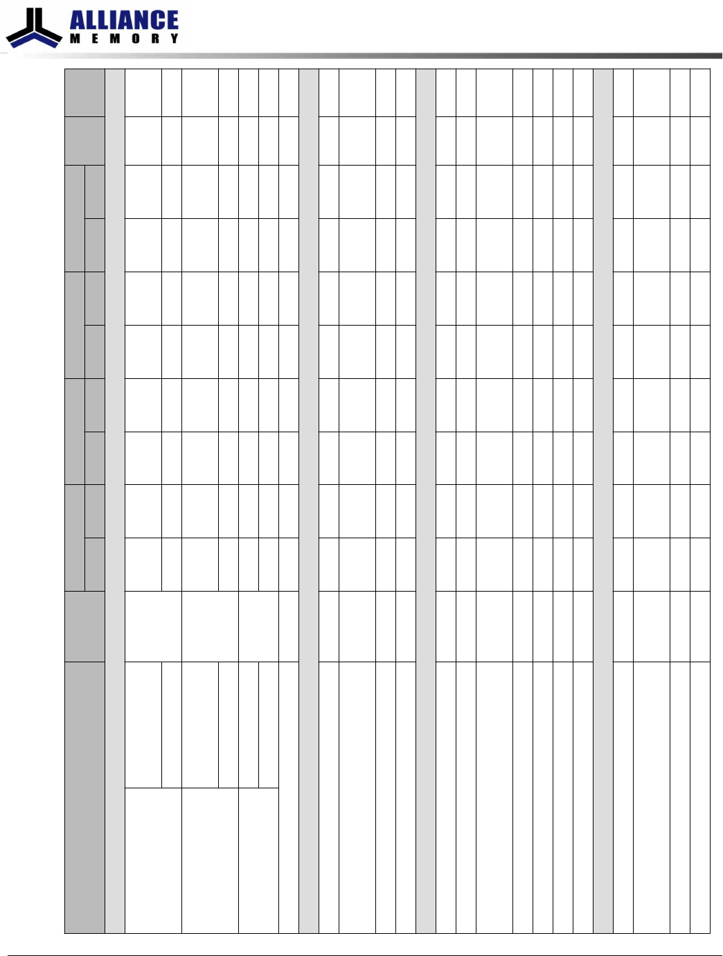
Table 55: Electrical Characteristics and AC Operating Conditions (Continued)
Notes 1–8 apply to the entire table
Parameter Symbol
DDR3L-800 DDR3L-1066 DDR3L-1333 DDR3L-1600
Unit NotesMin Max Min Max Min Max Min Max
DQ Input Timing
Data setup time to
DQS, DQS#
Base (specification)
t
DS
(AC160)
90 – 40 – – – – – ps 18, 19,
44
V
REF
@ 1 V/ns 250 – 200 – – – – – ps 19, 20
Data setup time to
DQS, DQS#
Base (specification)
t
DS
(AC135)
140 – 90 – 45 – 25 – ps 18, 19,
44
V
REF
@ 1 V/ns 275 – 250 – 180 – 160 – ps 19, 20
Data hold time from
DQS, DQS#
Base (specification)
t
DH
(DC90)
160 – 110 – 75 – 55 – ps 18, 19
V
REF
@ 1 V/ns 250 – 200 – 165 – 145 – ps 19, 20
Minimum data pulse width
t
DIPW 600 – 490 – 400 – 360 – ps 41
DQ Output Timing
DQS, DQS# to DQ skew, per access
t
DQSQ – 200 – 150 – 125 – 100 ps
DQ output hold time from DQS, DQS#
t
QH 0.38 – 0.38 – 0.38 – 0.38 –
t
CK
(AVG)
21
DQ Low-Z time from CK, CK#
t
LZDQ –800 400 –600 300 –500 250 –450 225 ps 22, 23
DQ High-Z time from CK, CK#
t
HZDQ – 400 – 300 – 250 – 225 ps 22, 23
DQ Strobe Input Timing
DQS, DQS# rising to CK, CK# rising
t
DQSS –0.25 0.25 –0.25 0.25 –0.25 0.25 –0.27 0.27 CK 25
DQS, DQS# differential input low pulse width
t
DQSL 0.45 0.55 0.45 0.55 0.45 0.55 0.45 0.55 CK
DQS, DQS# differential input high pulse
width
t
DQSH 0.45 0.55 0.45 0.55 0.45 0.55 0.45 0.55 CK
DQS, DQS# falling setup to CK, CK# rising
t
DSS 0.2 – 0.2 – 0.2 – 0.18 – CK 25
DQS, DQS# falling hold from CK, CK# rising
t
DSH 0.2 – 0.2 – 0.2 – 0.18 – CK 25
DQS, DQS# differential WRITE preamble
t
WPRE 0.9 – 0.9 – 0.9 – 0.9 – CK
DQS, DQS# differential WRITE postamble
t
WPST 0.3 – 0.3 – 0.3 – 0.3 – CK
DQ Strobe Output Timing
DQS, DQS# rising to/from rising CK, CK#
t
DQSCK –400 400 –300 300 –255 255 –225 225 ps 23
DQS, DQS# rising to/from rising CK, CK#
when DLL is disabled
t
DQSCK
(DLL_DIS)
110110110110ns26
DQS, DQS# differential output high time
t
QSH 0.38 – 0.38 – 0.40 – 0.40 – CK 21
DQS, DQS# differential output low time
t
QSL 0.38 – 0.38 – 0.40 – 0.40 – CK 21
8Gb: x4, x8, x16 DDR3L SDRAM
Electrical Characteristics and AC Operating Conditions
74
Rev 2.0 June 2016
© 2015 Alliance Memory, Inc. All rights reserved.
Alliance Memory Inc. reserves the right to change products or specification without notice
Alliance Memory Inc. 511 Taylor Way, San Carlos, CA 94070
TEL: (650) 610-6800 FAX: (650) 620-9211