
Datasheet
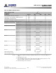
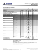
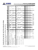

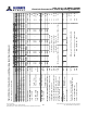
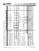
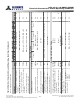
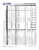
Table Of Contents
- DDR3L SDRAM
- Description
- State Diagram
- Functional Description
- Functional Block Diagrams
- Ball Assignments and Descriptions
- Package Dimensions
- Electrical Specifications
- Thermal Characteristics
- Electrical Specifications – I DD Specifications and Conditions
- Electrical Characteristics – 1.35V IDD Specifications
- Electrical Specifications – DC and AC
- ODT Characteristics
- Output Driver Impedance
- Output Characteristics and Operating Conditions
- Speed Bin Tables
- Electrical Characteristics and AC Operating Conditions
- Electrical Characteristics and AC Operating Conditions
- Command and Address Setup, Hold, and Derating
- Data Setup, Hold, and Derating
- Commands – Truth Tables
- Commands
- Input Clock Frequency Change
- Write Leveling
- Initialization
- Voltage Initialization / Change
- Mode Registers
- Mode Register 0 (MR0)
- Mode Register 1 (MR1)
- Mode Register 2 (MR2)
- Mode Register 3 (MR3)
- MODE REGISTER SET (MRS) Command
- ZQ CALIBRATION Operation
- ACTIVATE Operation
- READ Operation
- WRITE Operation
- PRECHARGE Operation
- SELF REFRESH Operation
- Extended Temperature Usage
- Power-Down Mode
- RESET Operation
- On-Die Termination (ODT)
- Dynamic ODT
- Synchronous ODT Mode
- Asynchronous ODT Mode
- Asynchronous to Synchronous ODT Mode Transition (Power-Down Exit)
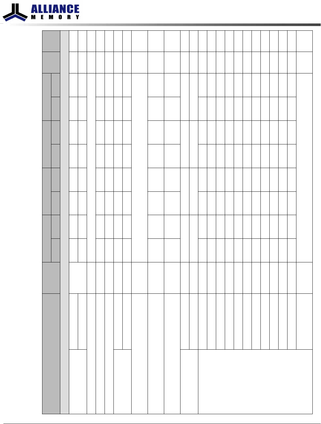
Electrical Characteristics and AC Operating Conditions
Table 55: Electrical Characteristics and AC Operating Conditions
Notes 1–8 apply to the entire table
Parameter Symbol
DDR3L-800 DDR3L-1066 DDR3L-1333 DDR3L-1600
Unit NotesMin Max Min Max Min Max Min Max
Clock Timing
Clock period average:
DLL disable mode
T
C
≤ 85°C
t
CK
(DLL_DIS)
8 7800 8 7800 8 7800 8 7800 ns 9, 42
T
C
= >85°C to 95°C 8 3900 8 3900 8 3900 8 3900 ns 42
Clock period average: DLL enable mode
t
CK (AVG) See Speed Bin Tables for
t
CK range allowed ns 10, 11
High pulse width average
t
CH (AVG) 0.47 0.53 0.47 0.53 0.47 0.53 0.47 0.53 CK 12
Low pulse width average
t
CL (AVG) 0.47 0.53 0.47 0.53 0.47 0.53 0.47 0.53 CK 12
Clock period jitter DLL locked
t
JITper –100 100 –90 90 –80 80 –70 70 ps 13
DLL locking
t
JITper,lck –90 90 –80 80 –70 70 –60 60 ps 13
Clock absolute period
t
CK (ABS) MIN =
t
CK (AVG) MIN +
t
JITper MIN; MAX =
t
CK (AVG) MAX +
t
JITper
MAX
ps
Clock absolute high pulse width
t
CH (ABS) 0.43 – 0.43 – 0.43 – 0.43 –
t
CK
(AVG)
14
Clock absolute low pulse width
t
CL (ABS) 0.43 – 0.43 – 0.43 – 0.43 –
t
CK
(AVG)
15
Cycle-to-cycle jitter DLL locked
t
JITcc 200 180 160 140 ps 16
DLL locking
t
JITcc,lck 180 160 140 120 ps 16
Cumulative error across 2 cycles
t
ERR2per –147 147 –132 132 –118 118 –103 103 ps 17
3 cycles
t
ERR3per –175 175 –157 157 –140 140 –122 122 ps 17
4 cycles
t
ERR4per –194 194 –175 175 –155 155 –136 136 ps 17
5 cycles
t
ERR5per –209 209 –188 188 –168 168 –147 147 ps 17
6 cycles
t
ERR6per –222 222 –200 200 –177 177 –155 155 ps 17
7 cycles
t
ERR7per –232 232 –209 209 –186 186 –163 163 ps 17
8 cycles
t
ERR8per –241 241 –217 217 –193 193 –169 169 ps 17
9 cycles
t
ERR9per –249 249 –224 224 –200 200 –175 175 ps 17
10 cycles
t
ERR10per –257 257 –231 231 –205 205 –180 180 ps 17
11 cycles
t
ERR11per –263 263 –237 237 –210 210 –184 184 ps 17
12 cycles
t
ERR12per –269 269 –242 242 –215 215 –188 188 ps 17
n = 13, 14 . . . 49, 50
cycles
t
ERRnper
t
ERRnper MIN = (1 + 0.68ln[n]) ×
t
JITper MIN
t
ERRnper MAX = (1 + 0.68ln[n]) ×
t
JITper MAX
ps 17
8Gb: x4, x8, x16 DDR3L SDRAM
Electrical Characteristics and AC Operating Conditions
73
Rev 2.0 June 2016
© 2015 Alliance Memory, Inc. All rights reserved.
Alliance Memory Inc. reserves the right to change products or specification without notice
Alliance Memory Inc. 511 Taylor Way, San Carlos, CA 94070
TEL: (650) 610-6800 FAX: (650) 620-9211