
Datasheet
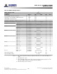
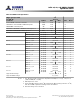
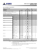
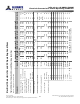

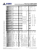
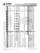
Table Of Contents
- DDR3L SDRAM
- Description
- State Diagram
- Functional Description
- Functional Block Diagrams
- Ball Assignments and Descriptions
- Package Dimensions
- Electrical Specifications
- Thermal Characteristics
- Electrical Specifications – I DD Specifications and Conditions
- Electrical Characteristics – 1.35V IDD Specifications
- Electrical Specifications – DC and AC
- ODT Characteristics
- Output Driver Impedance
- Output Characteristics and Operating Conditions
- Speed Bin Tables
- Electrical Characteristics and AC Operating Conditions
- Electrical Characteristics and AC Operating Conditions
- Command and Address Setup, Hold, and Derating
- Data Setup, Hold, and Derating
- Commands – Truth Tables
- Commands
- Input Clock Frequency Change
- Write Leveling
- Initialization
- Voltage Initialization / Change
- Mode Registers
- Mode Register 0 (MR0)
- Mode Register 1 (MR1)
- Mode Register 2 (MR2)
- Mode Register 3 (MR3)
- MODE REGISTER SET (MRS) Command
- ZQ CALIBRATION Operation
- ACTIVATE Operation
- READ Operation
- WRITE Operation
- PRECHARGE Operation
- SELF REFRESH Operation
- Extended Temperature Usage
- Power-Down Mode
- RESET Operation
- On-Die Termination (ODT)
- Dynamic ODT
- Synchronous ODT Mode
- Asynchronous ODT Mode
- Asynchronous to Synchronous ODT Mode Transition (Power-Down Exit)
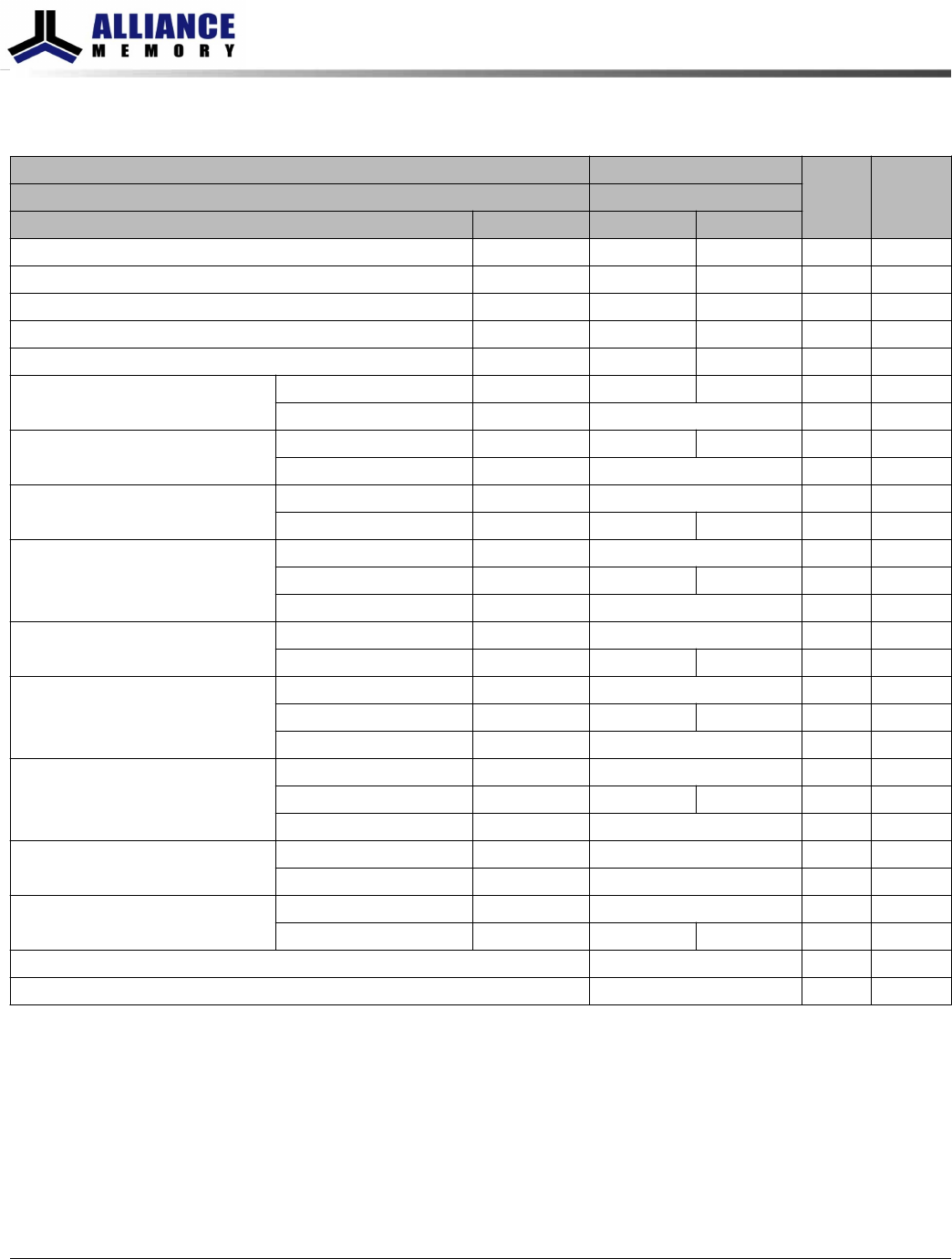
Table 53: DDR3L-1866 Speed Bins
DDR3L-1866 Speed Bin
-10
1
Unit Notes
CL-
t
RCD-
t
RP 13-13-13
Parameter Symbol Min Max
Internal READ command to first data
t
AA 13.91 20
ACTIVATE to internal READ or WRITE delay time
t
RCD 13.91 – ns
PRECHARGE command period
t
RP 13.91 – ns
ACTIVATE-to-ACTIVATE or REFRESH command period
t
RC 47.91 – ns
ACTIVATE-to-PRECHARGE command period
t
RAS 34 9 x
t
REFI ns 2
CL = 5 CWL = 5
t
CK (AVG) 3.0 3.3 ns 3
CWL = 6, 7, 8, 9
t
CK (AVG) Reserved ns 4
CL = 6 CWL = 5
t
CK (AVG) 2.5 3.3 ns 3
CWL = 6, 7, 8, 9
t
CK (AVG) Reserved ns 4
CL = 7 CWL = 5, 7, 8, 9
t
CK (AVG) Reserved ns 4
CWL = 6
t
CK (AVG) 1.875 <2.5 ns 3
CL = 8 CWL = 5, 8, 9
t
CK (AVG) Reserved ns 4
CWL = 6
t
CK (AVG) 1.875 <2.5 ns 3
CWL = 7
t
CK (AVG) Reserved ns 4
CL = 9 CWL = 5, 6, 8, 9
t
CK (AVG) Reserved ns 4
CWL = 7
t
CK (AVG) 1.5 <1.875 ns 3
CL = 10 CWL = 5, 6, 9
t
CK (AVG) Reserved ns 4
CWL = 7
t
CK (AVG) 1.5 <1.875 ns 3
CWL = 8
t
CK (AVG) Reserved ns 4
CL = 11 CWL = 5, 6, 7
t
CK (AVG) Reserved ns 4
CWL = 8
t
CK (AVG) 1.25 <1.5 ns 3
CWL = 9
t
CK (AVG) Reserved ns 4
CL = 12 CWL = 5, 6, 7, 8
t
CK (AVG) Reserved ns 4
CWL = 9
t
CK (AVG) Reserved ns 4
CL = 13 CWL = 5, 6, 7, 8
t
CK (AVG) Reserved ns 4
CWL = 9
t
CK (AVG) 1.07 <1.25 ns 3
Supported CL settings 5, 6, 7, 8, 9, 10, 11, 13 CK
Supported CWL settings 5, 6, 7, 8, 9 CK
Notes:
1.
The -107 speed grade is backward compatible with 1600, CL = 11 (-12) , 1333, CL = 9
(-15E) and 1066, CL = 7 (-18E).
2.
t
REFI depends on T
OPER
.
3. The CL and CWL settings result in
t
CK requirements. When making a selection of
t
CK,
both CL and CWL requirement settings need to be fulfilled.
4. Reserved settings are not allowed.
8Gb: x4, x8, x16 DDR3L SDRAM
Speed Bin Tables
71
Rev 2.0 June 2016
© 2015 Alliance Memory, Inc. All rights reserved.
Alliance Memory Inc. reserves the right to change products or specification without notice
Alliance Memory Inc. 511 Taylor Way, San Carlos, CA 94070
TEL: (650) 610-6800 FAX: (650) 620-9211