
Datasheet

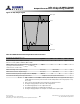
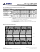


Table Of Contents
- DDR3L SDRAM
- Description
- State Diagram
- Functional Description
- Functional Block Diagrams
- Ball Assignments and Descriptions
- Package Dimensions
- Electrical Specifications
- Thermal Characteristics
- Electrical Specifications – I DD Specifications and Conditions
- Electrical Characteristics – 1.35V IDD Specifications
- Electrical Specifications – DC and AC
- ODT Characteristics
- Output Driver Impedance
- Output Characteristics and Operating Conditions
- Speed Bin Tables
- Electrical Characteristics and AC Operating Conditions
- Electrical Characteristics and AC Operating Conditions
- Command and Address Setup, Hold, and Derating
- Data Setup, Hold, and Derating
- Commands – Truth Tables
- Commands
- Input Clock Frequency Change
- Write Leveling
- Initialization
- Voltage Initialization / Change
- Mode Registers
- Mode Register 0 (MR0)
- Mode Register 1 (MR1)
- Mode Register 2 (MR2)
- Mode Register 3 (MR3)
- MODE REGISTER SET (MRS) Command
- ZQ CALIBRATION Operation
- ACTIVATE Operation
- READ Operation
- WRITE Operation
- PRECHARGE Operation
- SELF REFRESH Operation
- Extended Temperature Usage
- Power-Down Mode
- RESET Operation
- On-Die Termination (ODT)
- Dynamic ODT
- Synchronous ODT Mode
- Asynchronous ODT Mode
- Asynchronous to Synchronous ODT Mode Transition (Power-Down Exit)
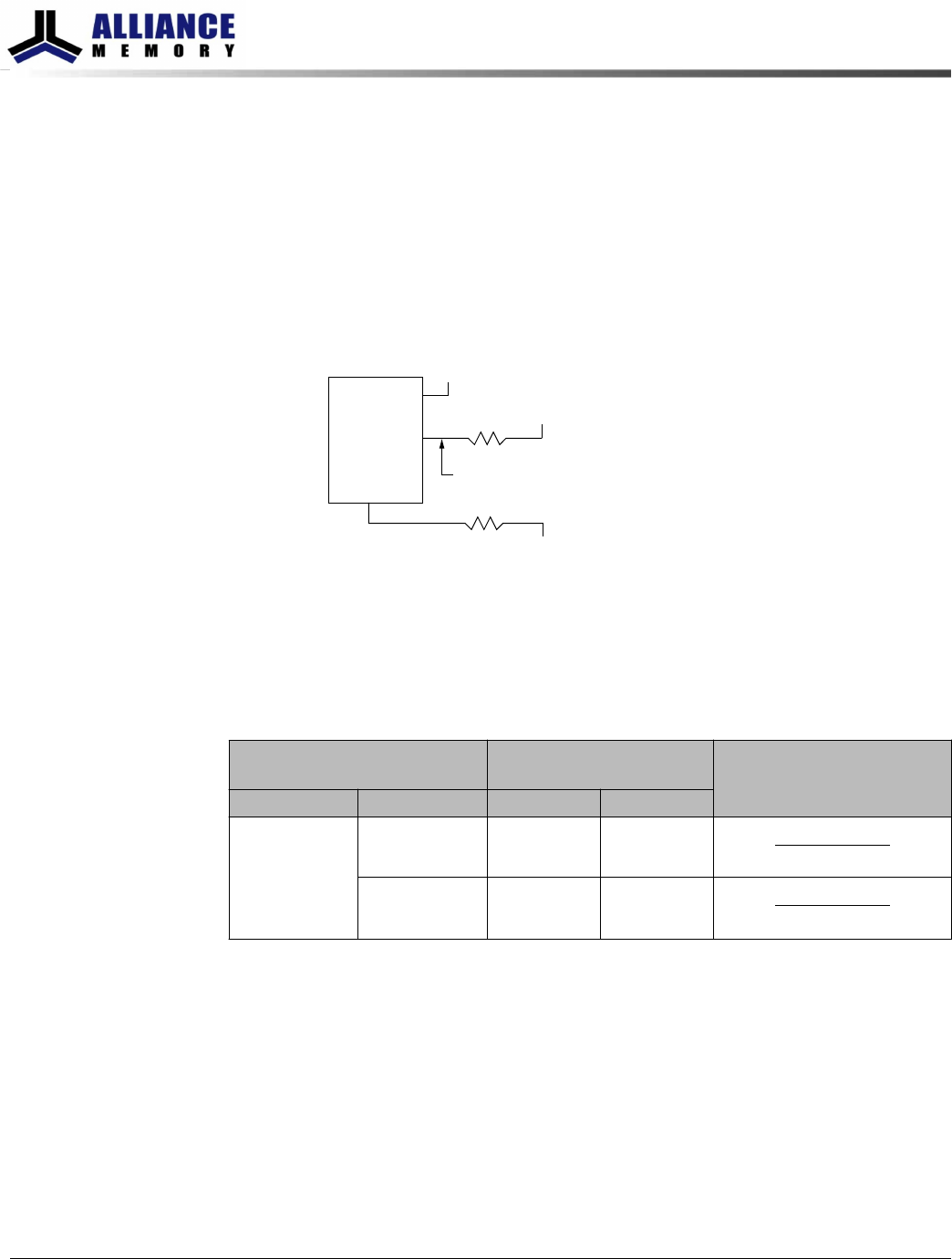
Reference Output Load
Figure 27 (page 65) represents the effective reference load of 25Ω used in defining the
relevant device AC timing parameters (except ODT reference timing) as well as the out-
put slew rate measurements. It is not intended to be a precise representation of a partic-
ular system environment or a depiction of the actual load presented by a production
tester. System designers should use IBIS or other simulation tools to correlate the tim-
ing reference load to a system environment.
Figure 27: Reference Output Load for AC Timing and Output Slew Rate
Timing reference point
DQ
DQS
DQS#
DUT
V
REF
V
TT
= V
DDQ
/2
V
DDQ
/2
ZQ
RZQ = 240ȍ
V
SS
R
TT
= 25ȍ
Slew Rate Definitions for Single-Ended Output Signals
The single-ended output driver is summarized in Table 45 (page 62). With the reference
load for timing measurements, the output slew rate for falling and rising edges is de-
fined and measured between V
OL(AC)
and V
OH(AC)
for single-ended signals.
Table 48: Single-Ended Output Slew Rate Definition
Single-Ended Output Slew
Rates (Linear Signals)
Measured
CalculationOutput Edge From To
DQ Rising V
OL(AC)
V
OH(AC)
V
OH(AC)
- V
OL(AC)
ΔTR
se
Falling V
OH(AC)
V
OL(AC)
V
OH(AC)
- V
OL(AC)
ΔTF
se
8Gb: x4, x8, x16 DDR3L SDRAM
Output Characteristics and Operating Conditions
65
Rev 2.0 June 2016
© 2015 Alliance Memory, Inc. All rights reserved.
Alliance Memory Inc. reserves the right to change products or specification without notice
Alliance Memory Inc. 511 Taylor Way, San Carlos, CA 94070
TEL: (650) 610-6800 FAX: (650) 620-9211