
Datasheet
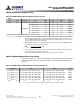
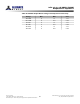

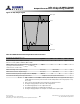


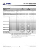
Table Of Contents
- DDR3L SDRAM
- Description
- State Diagram
- Functional Description
- Functional Block Diagrams
- Ball Assignments and Descriptions
- Package Dimensions
- Electrical Specifications
- Thermal Characteristics
- Electrical Specifications – I DD Specifications and Conditions
- Electrical Characteristics – 1.35V IDD Specifications
- Electrical Specifications – DC and AC
- ODT Characteristics
- Output Driver Impedance
- Output Characteristics and Operating Conditions
- Speed Bin Tables
- Electrical Characteristics and AC Operating Conditions
- Electrical Characteristics and AC Operating Conditions
- Command and Address Setup, Hold, and Derating
- Data Setup, Hold, and Derating
- Commands – Truth Tables
- Commands
- Input Clock Frequency Change
- Write Leveling
- Initialization
- Voltage Initialization / Change
- Mode Registers
- Mode Register 0 (MR0)
- Mode Register 1 (MR1)
- Mode Register 2 (MR2)
- Mode Register 3 (MR3)
- MODE REGISTER SET (MRS) Command
- ZQ CALIBRATION Operation
- ACTIVATE Operation
- READ Operation
- WRITE Operation
- PRECHARGE Operation
- SELF REFRESH Operation
- Extended Temperature Usage
- Power-Down Mode
- RESET Operation
- On-Die Termination (ODT)
- Dynamic ODT
- Synchronous ODT Mode
- Asynchronous ODT Mode
- Asynchronous to Synchronous ODT Mode Transition (Power-Down Exit)
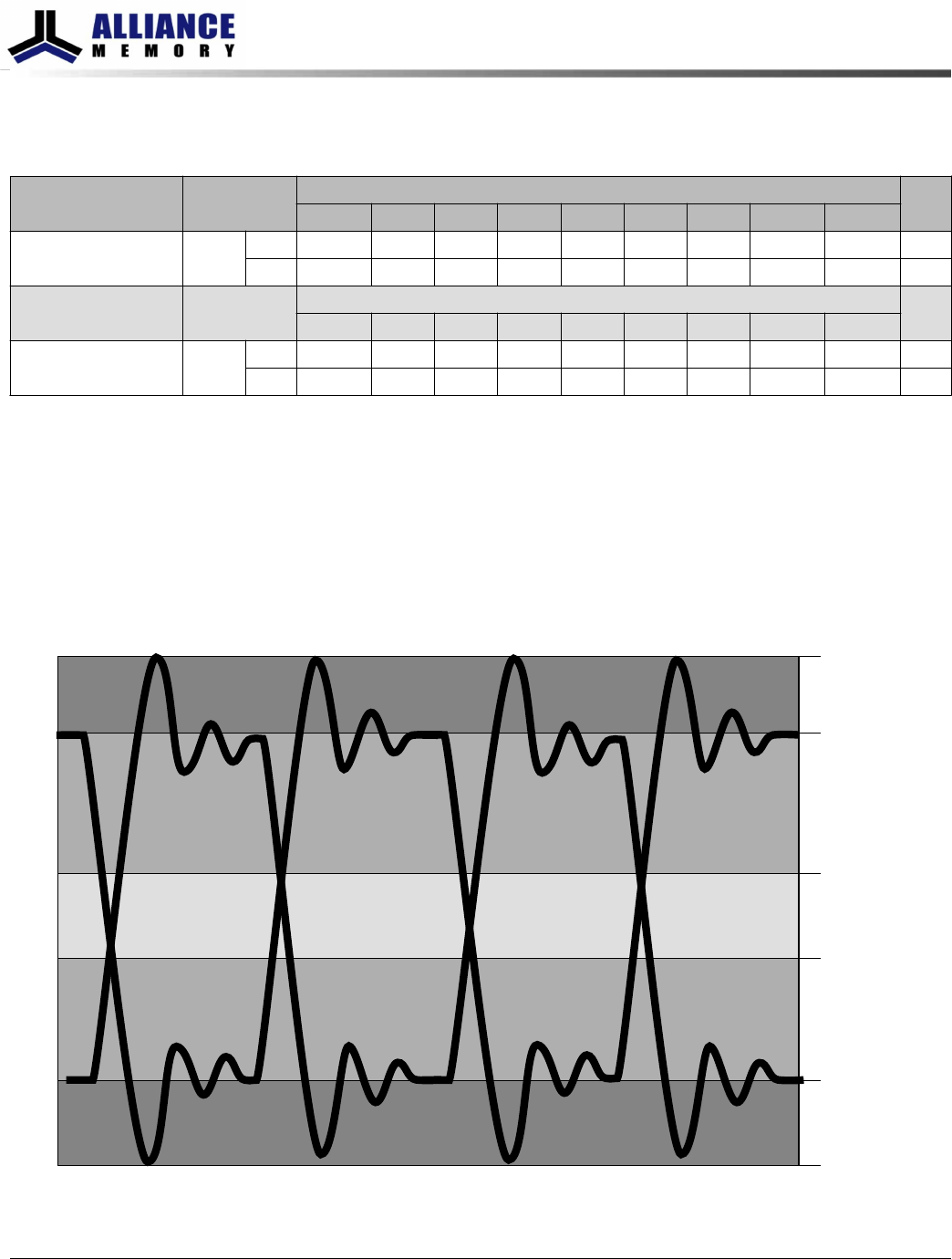
Table 47: DDR3L Differential Output Driver Characteristics V
OX(AC)
All voltages are referenced to V
SS
Parameter/
Condition
Symbol
DDR3L- 800/1066/1333 DQS/DQS# Differential Slew Rate
Unit
3.5V/ns 4V/ns 5V/ns 6V/ns 7V/ns 8V/ns 9V/ns 10V/ns 12V/ns
Output differential
crosspoint voltage
V
OX(AC)
Max 115 130 135 195 205 205 205 205 205 mV
Min –115 –130 –135 –195 –205 –205 –205 –205 –205 mV
Parameter/
Condition
Symbol
DDR3L-1600/1866/2133 DQS/DQS# Differential Slew Rate
Unit
3.5V/ns 4V/ns 5v/ns 6V/ns 7V/ns 8V/ns 9V/ns 10V/ns 12V/ns
Output differential
crosspoint voltage
V
OX(AC)
Max 90 105 135 155 180 205 205 205 205 mV
Min –90 –105 –135 –155 –180 –205 –205 –205 –205 mV
Notes:
1. RZQ of 240Ω ±1% with RZQ/7 enabled (default 34Ω driver) and is applicable after prop-
er ZQ calibration has been performed at a stable temperature and voltage (V
DDQ
= V
DD
;
V
SSQ
= V
SS
).
2. See Figure 27 (page 65) for the test load configuration.
3. See Figure 26 (page 64) for an example of a differential output signal.
4. For a differential slew rate between the list values, the V
OX(AC)
value may be obtained
by linear interpolation.
Figure 26: Differential Output Signal
V
OH
MIN output
MAX output
V
OL
V
OX(AC)max
V
OX(AC)min
X
X
X
X
8Gb: x4, x8, x16 DDR3L SDRAM
Output Characteristics and Operating Conditions
64
Rev 2.0 June 2016
© 2015 Alliance Memory, Inc. All rights reserved.
Alliance Memory Inc. reserves the right to change products or specification without notice
Alliance Memory Inc. 511 Taylor Way, San Carlos, CA 94070
TEL: (650) 610-6800 FAX: (650) 620-9211