
Datasheet
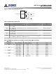

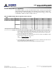

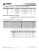
Table Of Contents
- DDR3L SDRAM
- Description
- State Diagram
- Functional Description
- Functional Block Diagrams
- Ball Assignments and Descriptions
- Package Dimensions
- Electrical Specifications
- Thermal Characteristics
- Electrical Specifications – I DD Specifications and Conditions
- Electrical Characteristics – 1.35V IDD Specifications
- Electrical Specifications – DC and AC
- ODT Characteristics
- Output Driver Impedance
- Output Characteristics and Operating Conditions
- Speed Bin Tables
- Electrical Characteristics and AC Operating Conditions
- Electrical Characteristics and AC Operating Conditions
- Command and Address Setup, Hold, and Derating
- Data Setup, Hold, and Derating
- Commands – Truth Tables
- Commands
- Input Clock Frequency Change
- Write Leveling
- Initialization
- Voltage Initialization / Change
- Mode Registers
- Mode Register 0 (MR0)
- Mode Register 1 (MR1)
- Mode Register 2 (MR2)
- Mode Register 3 (MR3)
- MODE REGISTER SET (MRS) Command
- ZQ CALIBRATION Operation
- ACTIVATE Operation
- READ Operation
- WRITE Operation
- PRECHARGE Operation
- SELF REFRESH Operation
- Extended Temperature Usage
- Power-Down Mode
- RESET Operation
- On-Die Termination (ODT)
- Dynamic ODT
- Synchronous ODT Mode
- Asynchronous ODT Mode
- Asynchronous to Synchronous ODT Mode Transition (Power-Down Exit)
Table 39: DDR3L 34 Ohm Driver I
OH
/I
OL
Characteristics: V
DD
= V
DDQ
= DDR3L@1.283
MR1[5,1] R
ON
Resistor V
OUT
Max Nom Min Unit
0, 1 Ω R
ON34(PD)
I
OL
@ 0.2 × V
DDQ
12.6 7.5 6.7 mA
I
OL
@ 0.5 × V
DDQ
21.0 18.7 16.8 mA
I
OL
@ 0.8 × V
DDQ
33.6 29.9 21.2 mA
R
ON34(PU)
I
OH
@ 0.2 × V
DDQ
33.6 29.9 21.2 mA
I
OH
@ 0.5 × V
DDQ
21.0 18.7 16.8 mA
I
OH
@ 0.8 × V
DDQ
12.6 7.5 6.7 mA
DDR3L 34 Ohm Output Driver Sensitivity
If either the temperature or the voltage changes after ZQ calibration, then the tolerance
limits listed in Table 35 (page 57) can be expected to widen according to Table 40 and
Table 41.
Table 40: DDR3L 34 Ohm Output Driver Sensitivity Definition
Symbol Min Max Unit
R
ON(PD)
@ 0.2 × V
DDQ
0.6 - dR
ON
dTL × |ΔT| - dR
ON
dVL × |ΔV| 1.1 + dR
ON
dTL × |ΔT| + dR
ON
dVL × |ΔV| RZQ/7
R
ON(PD)
@ 0.5 × V
DDQ
0.9 - dR
ON
dTM × |ΔT| - dR
ON
dVM × |ΔV| 1.1 + dR
ON
dTM × |ΔT| + dR
ON
dVM × |ΔV| RZQ/7
R
ON(PD)
@ 0.8 × V
DDQ
0.9 - dR
ON
dTH × |ΔT| - dR
ON
dVH × |ΔV| 1.4 + dR
ON
dTH × |ΔT| + dR
ON
dVH × |ΔV| RZQ/7
R
ON(PU)
@ 0.2 × V
DDQ
0.9 - dR
ON
dTL × |ΔT| - dR
ON
dVL × |ΔV| 1.4 + dR
ON
dTL × |ΔT| + dR
ON
dVL × |ΔV| RZQ/7
R
ON(PU)
@ 0.5 × V
DDQ
0.9 - dR
ON
dTM × |ΔT| - dR
ON
dVM × |ΔV| 1.1 + dR
ON
dTM × |ΔT| + dR
ON
dVM × |ΔV| RZQ/7
R
ON(PU)
@ 0.8 × V
DDQ
0.6 - dR
ON
dTH × |ΔT| - dR
ON
dVH × |ΔV| 1.1 + dR
ON
dTH × |ΔT| + dR
ON
dVH × |ΔV| RZQ/7
Note:
1. ΔT = T - T
(@CALIBRATION)
ΔV = V
DDQ
- V
DDQ(@CALIBRATION)
; and V
DD
= V
DDQ
.
Table 41: DDR3L 34 Ohm Output Driver Voltage and Temperature Sensitivity
Change Min Max Unit
dR
ON
dTM 0 1.5 %/°C
dR
ON
dVM 0 0.13 %/mV
dR
ON
dTL 0 1.5 %/°C
dR
ON
dVL 0 0.13 %/mV
dR
ON
dTH 0 1.5 %/°C
dR
ON
dVH 0 0.13 %/mV
8Gb: x4, x8, x16 DDR3L SDRAM
Output Driver Impedance
59
Rev 2.0 June 2016
© 2015 Alliance Memory, Inc. All rights reserved.
Alliance Memory Inc. reserves the right to change products or specification without notice
Alliance Memory Inc. 511 Taylor Way, San Carlos, CA 94070
TEL: (650) 610-6800 FAX: (650) 620-9211