
Datasheet
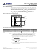
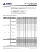

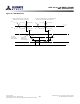
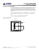

Table Of Contents
- DDR3L SDRAM
- Description
- State Diagram
- Functional Description
- Functional Block Diagrams
- Ball Assignments and Descriptions
- Package Dimensions
- Electrical Specifications
- Thermal Characteristics
- Electrical Specifications – I DD Specifications and Conditions
- Electrical Characteristics – 1.35V IDD Specifications
- Electrical Specifications – DC and AC
- ODT Characteristics
- Output Driver Impedance
- Output Characteristics and Operating Conditions
- Speed Bin Tables
- Electrical Characteristics and AC Operating Conditions
- Electrical Characteristics and AC Operating Conditions
- Command and Address Setup, Hold, and Derating
- Data Setup, Hold, and Derating
- Commands – Truth Tables
- Commands
- Input Clock Frequency Change
- Write Leveling
- Initialization
- Voltage Initialization / Change
- Mode Registers
- Mode Register 0 (MR0)
- Mode Register 1 (MR1)
- Mode Register 2 (MR2)
- Mode Register 3 (MR3)
- MODE REGISTER SET (MRS) Command
- ZQ CALIBRATION Operation
- ACTIVATE Operation
- READ Operation
- WRITE Operation
- PRECHARGE Operation
- SELF REFRESH Operation
- Extended Temperature Usage
- Power-Down Mode
- RESET Operation
- On-Die Termination (ODT)
- Dynamic ODT
- Synchronous ODT Mode
- Asynchronous ODT Mode
- Asynchronous to Synchronous ODT Mode Transition (Power-Down Exit)
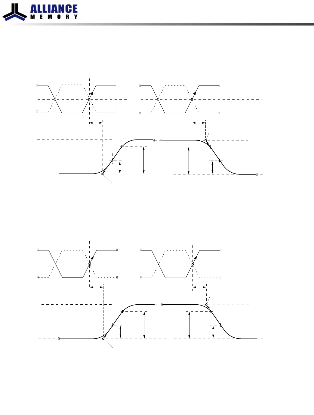
Figure 21:
t
AON and
t
AOF Definitions
CK
CK#
t
AON
V
SSQ
DQ, DM
DQS, DQS#
TDQS, TDQS#
Begin point: Rising edge of CK - CK#
defined by the end point of ODTLon
V
SW1
End point: Extrapolated point at V
SSQ
T
SW1
T
SW2
CK
CK#
V
DDQ
/2
t
AOF
Begin point: Rising edge of CK - CK#
defined by the end point of ODTLoff
End point: Extrapolated point at V
RTT,nom
V
RTT,nom
V
SSQ
t
AON
t
AOF
V
SW2
V
SW2
V
SW1
T
SW1
T
SW1
Figure 22:
t
AONPD and
t
AOFPD Definitions
CK
CK#
t
AONPD
V
SSQ
DQ, DM
DQS, DQS#
TDQS, TDQS#
Begin point: Rising edge of CK - CK#
with ODT first registered high
V
SW1
End point: Extrapolated point at V
SSQ
T
SW2
CK
CK#
V
DDQ
/2
t
AOFPD
Begin point: Rising edge of CK - CK#
with ODT first registered low
End point: Extrapolated point at V
RTT,nom
V
RTT,nom
V
SSQ
t
AONPD
t
AOFPD
T
SW1
T
SW2
T
SW1
V
SW2
V
SW2
V
SW1
8Gb: x4, x8, x16 DDR3L SDRAM
ODT Characteristics
54
Rev 2.0 June 2016
© 2015 Alliance Memory, Inc. All rights reserved.
Alliance Memory Inc. reserves the right to change products or specification without notice
Alliance Memory Inc. 511 Taylor Way, San Carlos, CA 94070
TEL: (650) 610-6800 FAX: (650) 620-9211