
Datasheet
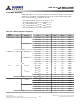
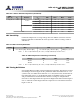
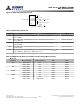

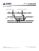
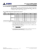

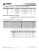
Table Of Contents
- DDR3L SDRAM
- Description
- State Diagram
- Functional Description
- Functional Block Diagrams
- Ball Assignments and Descriptions
- Package Dimensions
- Electrical Specifications
- Thermal Characteristics
- Electrical Specifications – I DD Specifications and Conditions
- Electrical Characteristics – 1.35V IDD Specifications
- Electrical Specifications – DC and AC
- ODT Characteristics
- Output Driver Impedance
- Output Characteristics and Operating Conditions
- Speed Bin Tables
- Electrical Characteristics and AC Operating Conditions
- Electrical Characteristics and AC Operating Conditions
- Command and Address Setup, Hold, and Derating
- Data Setup, Hold, and Derating
- Commands – Truth Tables
- Commands
- Input Clock Frequency Change
- Write Leveling
- Initialization
- Voltage Initialization / Change
- Mode Registers
- Mode Register 0 (MR0)
- Mode Register 1 (MR1)
- Mode Register 2 (MR2)
- Mode Register 3 (MR3)
- MODE REGISTER SET (MRS) Command
- ZQ CALIBRATION Operation
- ACTIVATE Operation
- READ Operation
- WRITE Operation
- PRECHARGE Operation
- SELF REFRESH Operation
- Extended Temperature Usage
- Power-Down Mode
- RESET Operation
- On-Die Termination (ODT)
- Dynamic ODT
- Synchronous ODT Mode
- Asynchronous ODT Mode
- Asynchronous to Synchronous ODT Mode Transition (Power-Down Exit)

Table 30: 1.35V R
TT
Effective Impedance (Continued)
MR1
[9, 6, 2]
R
TT
Resistor V
OUT
Min Nom Max Units
1, 0, 0 Ω R
TT,20PD40
0.2 × V
DDQ
0.6 1.0 1.15 RZQ/6
0.5 × V
DDQ
0.9 1.0 1.15 RZQ/6
0.8 × V
DDQ
0.9 1.0 1.45 RZQ/6
R
TT,20PU40
0.2 × V
DDQ
0.9 1.0 1.45 RZQ/6
0.5 × V
DDQ
0.9 1.0 1.15 RZQ/6
0.8 × V
DDQ
0.6 1.0 1.15 RZQ/6
Ω V
IL(AC)
to V
IH(AC)
0.9 1.0 1.65 RZQ/12
ODT Sensitivity
If either the temperature or voltage changes after I/O calibration, then the tolerance
limits listed in Table 29 and Table 30 can be expected to widen according to Table 31
and Table 32.
Table 31: ODT Sensitivity Definition
Symbol Min Max Unit
R
TT
0.9 - dR
TT
dT × |DT| - dR
TT
dV × |DV| 1.6 + dR
TT
dT × |DT| + dR
TT
dV × |DV| RZQ/(2, 4, 6, 8, 12)
Note:
1. ΔT = T - T(@ calibration), ΔV = V
DDQ
- V
DDQ
(@ calibration) and V
DD
= V
DDQ
.
Table 32: ODT Temperature and Voltage Sensitivity
Change Min Max Unit
dR
TT
dT 0 1.5 %/°C
dR
TT
dV 0 0.15 %/mV
Note:
1. ΔT = T - T(@ calibration), ΔV = V
DDQ
- V
DDQ
(@ calibration) and V
DD
= V
DDQ
.
ODT Timing Definitions
ODT loading differs from that used in AC timing measurements. The reference load for
ODT timings is shown in Figure 20. Two parameters define when ODT turns on or off
synchronously, two define when ODT turns on or off asynchronously, and another de-
fines when ODT turns on or off dynamically. Table 33 and Table 34 (page 53) outline
and provide definition and measurement references settings for each parameter.
ODT turn-on time begins when the output leaves High-Z and ODT resistance begins to
turn on. ODT turn-off time begins when the output leaves Low-Z and ODT resistance
begins to turn off.
8Gb: x4, x8, x16 DDR3L SDRAM
ODT Characteristics
52
Rev 2.0 June 2016
© 2015 Alliance Memory, Inc. All rights reserved.
Alliance Memory Inc. reserves the right to change products or specification without notice
Alliance Memory Inc. 511 Taylor Way, San Carlos, CA 94070
TEL: (650) 610-6800 FAX: (650) 620-9211