
Datasheet
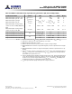
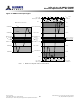
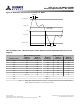
Table Of Contents
- DDR3L SDRAM
- Description
- State Diagram
- Functional Description
- Functional Block Diagrams
- Ball Assignments and Descriptions
- Package Dimensions
- Electrical Specifications
- Thermal Characteristics
- Electrical Specifications – I DD Specifications and Conditions
- Electrical Characteristics – 1.35V IDD Specifications
- Electrical Specifications – DC and AC
- ODT Characteristics
- Output Driver Impedance
- Output Characteristics and Operating Conditions
- Speed Bin Tables
- Electrical Characteristics and AC Operating Conditions
- Electrical Characteristics and AC Operating Conditions
- Command and Address Setup, Hold, and Derating
- Data Setup, Hold, and Derating
- Commands – Truth Tables
- Commands
- Input Clock Frequency Change
- Write Leveling
- Initialization
- Voltage Initialization / Change
- Mode Registers
- Mode Register 0 (MR0)
- Mode Register 1 (MR1)
- Mode Register 2 (MR2)
- Mode Register 3 (MR3)
- MODE REGISTER SET (MRS) Command
- ZQ CALIBRATION Operation
- ACTIVATE Operation
- READ Operation
- WRITE Operation
- PRECHARGE Operation
- SELF REFRESH Operation
- Extended Temperature Usage
- Power-Down Mode
- RESET Operation
- On-Die Termination (ODT)
- Dynamic ODT
- Synchronous ODT Mode
- Asynchronous ODT Mode
- Asynchronous to Synchronous ODT Mode Transition (Power-Down Exit)
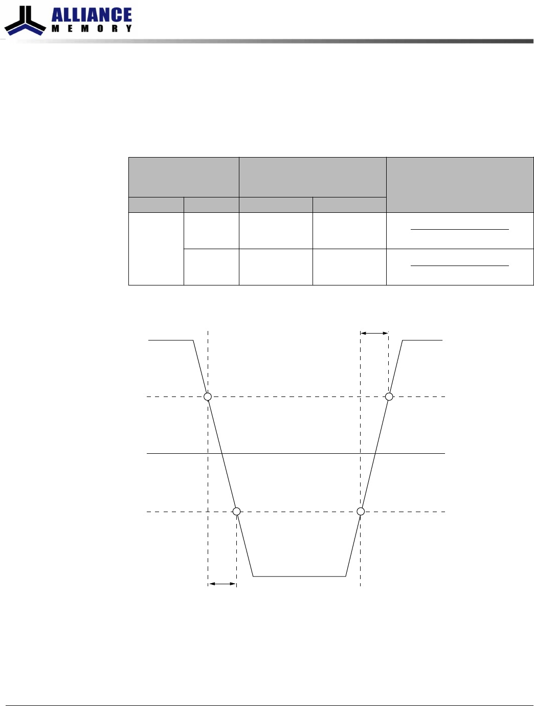
DDR3L 1.35V Slew Rate Definitions for Differential Input Signals
Input slew rate for differential signals (CK, CK# and DQS, DQS#) are defined and meas-
ured, as shown in Table 28 and Figure 18. The nominal slew rate for a rising signal is
defined as the slew rate between V
IL,diff,max
and V
IH,diff,min
. The nominal slew rate for a
falling signal is defined as the slew rate between V
IH,diff,min
and V
IL,diff,max
.
Table 28: DDR3L 1.35V Differential Input Slew Rate Definition
Differential Input
Slew Rates
(Linear Signals)
Measured
CalculationInput Edge From To
CK and
DQS
reference
Rising V
IL,diff,max
V
IH,diff,min
V
IH,diff,min
- V
IL,diff,max
ΔTR
diff
Falling V
IH,diff,min
V
IL,diff,max
V
IH,diff,min
- V
IL,diff,max
ΔTF
diff
Figure 18: DDR3L 1.35V Nominal Differential Input Slew Rate Definition for DQS, DQS# and CK, CK#
ΔTR
diff
ΔTF
diff
V
IH,diff,min
V
IL,diff,max
0
Differential input voltage (DQS, DQS#; CK, CK#)
8Gb: x4, x8, x16 DDR3L SDRAM
Electrical Specifications – DC and AC
49
Rev 2.0 June 2016
© 2015 Alliance Memory, Inc. All rights reserved.
Alliance Memory Inc. reserves the right to change products or specification without notice
Alliance Memory Inc. 511 Taylor Way, San Carlos, CA 94070
TEL: (650) 610-6800 FAX: (650) 620-9211