
Datasheet
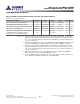
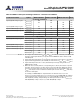
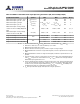
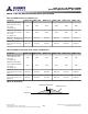
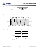
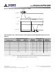
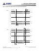
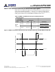
Table Of Contents
- DDR3L SDRAM
- Description
- State Diagram
- Functional Description
- Functional Block Diagrams
- Ball Assignments and Descriptions
- Package Dimensions
- Electrical Specifications
- Thermal Characteristics
- Electrical Specifications – I DD Specifications and Conditions
- Electrical Characteristics – 1.35V IDD Specifications
- Electrical Specifications – DC and AC
- ODT Characteristics
- Output Driver Impedance
- Output Characteristics and Operating Conditions
- Speed Bin Tables
- Electrical Characteristics and AC Operating Conditions
- Electrical Characteristics and AC Operating Conditions
- Command and Address Setup, Hold, and Derating
- Data Setup, Hold, and Derating
- Commands – Truth Tables
- Commands
- Input Clock Frequency Change
- Write Leveling
- Initialization
- Voltage Initialization / Change
- Mode Registers
- Mode Register 0 (MR0)
- Mode Register 1 (MR1)
- Mode Register 2 (MR2)
- Mode Register 3 (MR3)
- MODE REGISTER SET (MRS) Command
- ZQ CALIBRATION Operation
- ACTIVATE Operation
- READ Operation
- WRITE Operation
- PRECHARGE Operation
- SELF REFRESH Operation
- Extended Temperature Usage
- Power-Down Mode
- RESET Operation
- On-Die Termination (ODT)
- Dynamic ODT
- Synchronous ODT Mode
- Asynchronous ODT Mode
- Asynchronous to Synchronous ODT Mode Transition (Power-Down Exit)
DDR3L 1.35V AC Overshoot/Undershoot Specification
Table 24: DDR3L Control and Address Pins
Parameter DDR3L-800 DRR3L-1066 DDR3L-1333 DDR3L-1600 DDR3L-1866 DDR3L-2133
Maximum peak ampli-
tude allowed for over-
shoot area
(see Figure 12)
0.4V 0.4V 0.4V 0.4V 0.4V 0.4V
Maximum peak ampli-
tude allowed for under-
shoot area
(see Figure 13)
0.4V 0.4V 0.4V 0.4V 0.4V 0.4V
Maximum overshoot area
above V
DD
(see Figure 12)
0.67 V/ns 0.5 V/ns 0.4 V/ns 0.33 V/ns 0.28 V/ns 0.25 V/ns
Maximum undershoot
area below V
SS
(see Fig-
ure 13)
0.67 V/ns 0.5 V/ns 0.4 V/ns 0.33 V/ns 0.28 V/ns 0.25 V/ns
Table 25: DDR3L 1.35V Clock, Data, Strobe, and Mask Pins
Parameter DDR3L-800 DDR3L-1066 DDR3L-1333 DDR3L-1600 DDR3L-1866 DDR3L-2133
Maximum peak ampli-
tude allowed for over-
shoot area
(see Figure 12)
0.4V 0.4V 0.4V 0.4V 0.4V 0.4V
Maximum peak ampli-
tude allowed for under-
shoot area
(see Figure 13)
0.4V 0.4V 0.4V 0.4V 0.4V 0.4V
Maximum overshoot area
above V
DD
/V
DDQ
(see Fig-
ure 12)
0.25 V/ns 0.19 V/ns 0.15 V/ns 0.13 V/ns 0.11 V/ns 0.10 V/ns
Maximum undershoot
area below V
SS
/V
SSQ
(see
Figure 13)
0.25 V/ns 0.19 V/ns 0.15 V/ns 0.13 V/ns 0.11 V/ns 0.10 V/ns
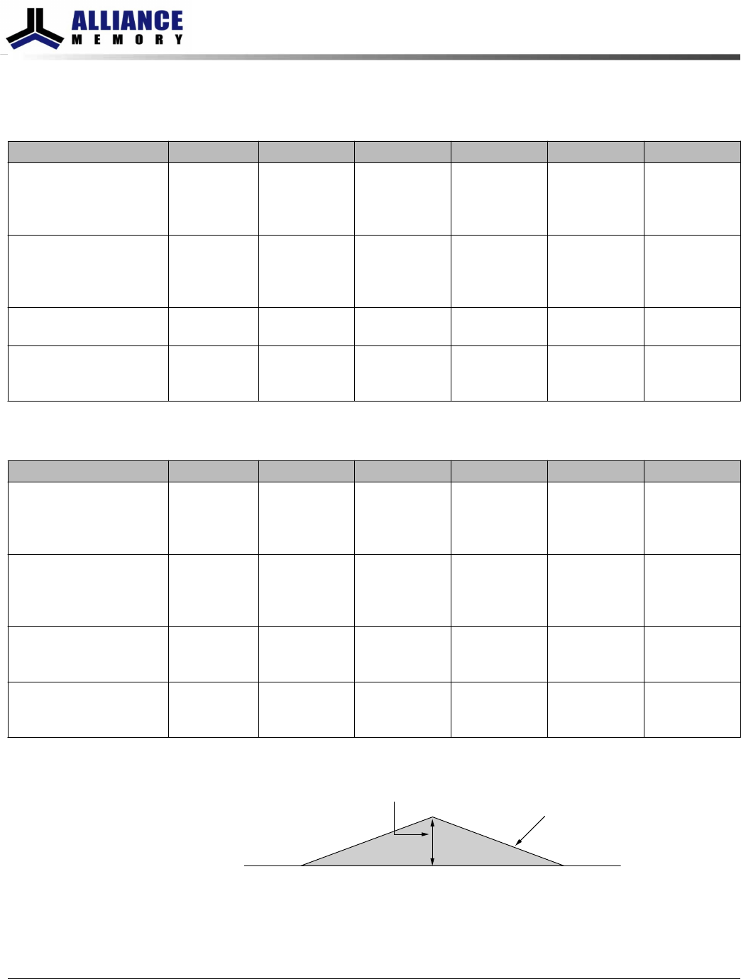
Figure 12: Overshoot
Maximum amplitude
Overshoot area
V
DD
/V
DDQ
Time (ns)
Volts (V)
8Gb: x4, x8, x16 DDR3L SDRAM
Electrical Specifications – DC and AC
44
Rev.2.0 June 2016
© 2015 Alliance Memory, Inc. All rights reserved.
Alliance Memory Inc. reserves the right to change products or specification without notice
Alliance Memory Inc. 511 Taylor Way, San Carlos, CA 94070
TEL: (650) 610-6800 FAX: (650) 620-9211