
Datasheet


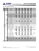
Table Of Contents
- DDR3L SDRAM
- Description
- State Diagram
- Functional Description
- Functional Block Diagrams
- Ball Assignments and Descriptions
- Package Dimensions
- Electrical Specifications
- Thermal Characteristics
- Electrical Specifications – I DD Specifications and Conditions
- Electrical Characteristics – 1.35V IDD Specifications
- Electrical Specifications – DC and AC
- ODT Characteristics
- Output Driver Impedance
- Output Characteristics and Operating Conditions
- Speed Bin Tables
- Electrical Characteristics and AC Operating Conditions
- Electrical Characteristics and AC Operating Conditions
- Command and Address Setup, Hold, and Derating
- Data Setup, Hold, and Derating
- Commands – Truth Tables
- Commands
- Input Clock Frequency Change
- Write Leveling
- Initialization
- Voltage Initialization / Change
- Mode Registers
- Mode Register 0 (MR0)
- Mode Register 1 (MR1)
- Mode Register 2 (MR2)
- Mode Register 3 (MR3)
- MODE REGISTER SET (MRS) Command
- ZQ CALIBRATION Operation
- ACTIVATE Operation
- READ Operation
- WRITE Operation
- PRECHARGE Operation
- SELF REFRESH Operation
- Extended Temperature Usage
- Power-Down Mode
- RESET Operation
- On-Die Termination (ODT)
- Dynamic ODT
- Synchronous ODT Mode
- Asynchronous ODT Mode
- Asynchronous to Synchronous ODT Mode Transition (Power-Down Exit)

Electrical Specifications – DC and AC
DC Operating Conditions
Table 20: DDR3L 1.35V DC Electrical Characteristics and Operating Conditions
All voltages are referenced to V
SS
Parameter/Condition Symbol Min Nom Max Unit Notes
Supply voltage V
DD
1.283 1.35 1.45 V 1–7
I/O supply voltage V
DDQ
1.283 1.35 1.45 V 1–7
Input leakage current
Any input 0V ≤ V
IN
≤ V
DD
, V
REF
pin 0V ≤ V
IN
≤ 1.1V
(All other pins not under test = 0V)
I
I
–2 – 2 μA
V
REF
supply leakage current
V
REFDQ
= V
DD
/2 or V
REFCA
= V
DD
/2
(All other pins not under test = 0V)
I
VREF
–1 – 1 μA 8, 9
Notes:
1. V
DD
and V
DDQ
must track one another. V
DDQ
must be ≤ V
DD
. V
SS
= V
SSQ
.
2. V
DD
and V
DDQ
may include AC noise of ±50mV (250 kHz to 20 MHz) in addition to the
DC (0 Hz to 250 kHz) specifications. V
DD
and V
DDQ
must be at same level for valid AC
timing parameters.
3. Maximum DC value may not be greater than 1.425V. The DC value is the linear average
of V
DD
/V
DDQ
(t) over a very long period of time (for example, 1 second).
4. Under these supply voltages, the device operates to this DDR3L specification.
5. If the maximum limit is exceeded, input levels shall be governed by DDR3 specifications.
6. Under 1.5V operation, this DDR3L device operates in accordance with the DDR3 specifi-
cations under the same speed timings as defined for this device.
7. Once initialized for DDR3L operation, DDR3 operation may only be used if the device is
in reset while V
DD
and V
DDQ
are changed for DDR3 operation (see V
DD
Voltage Switch-
ing (page 129)).
8. The minimum limit requirement is for testing purposes. The leakage current on the V
REF
pin should be minimal.
9. V
REF
(see Table 21).
8Gb: x4, x8, x16 DDR3L SDRAM
Electrical Specifications – DC and AC
39
Rev.2.0 June 2016
© 2015 Alliance Memory, Inc. All rights reserved.
Alliance Memory Inc. reserves the right to change products or specification without notice
Alliance Memory Inc. 511 Taylor Way, San Carlos, CA 94070
TEL: (650) 610-6800 FAX: (650) 620-9211